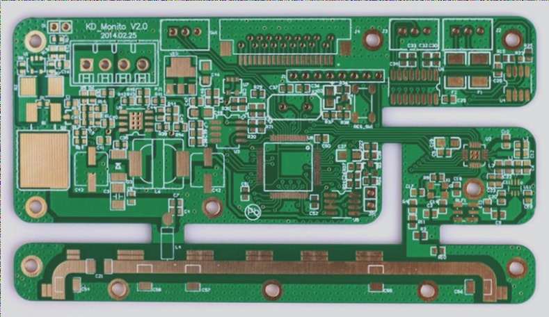
Component Arrangement Guidelines:
- Under normal conditions, all components should be placed on the same side of the PCB. Exceptions can be made for low-profile devices like chip resistors and capacitors when the top side is densely populated.
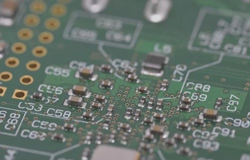
- Components should be arranged on a grid, parallel or perpendicular to each other for a neat appearance, avoiding overlap and maintaining compactness.
- High potential difference components should have increased spacing to prevent short circuits.
- Components operating at high voltage should be placed in less accessible areas during debugging.
- Components at the board edge should be at least two board thicknesses away from the edge.
- Components should be evenly distributed with uniform density across the board surface.

Layout Principles Based on Signal Direction:
- Position functional circuit units sequentially following signal flow for efficient layout.
- Facilitate consistent signal flow direction, typically from left to right or top to bottom.
- Place components near input and output terminals for better signal connectivity.
Preventing Electromagnetic Interference:
- Space components emitting strong electromagnetic fields apart and shield sensitive ones.
- Avoid mixing high and low voltage devices and separate strong and weak signal components.
- Minimize magnetic field interference and shield sources effectively with grounding.
Managing Thermal Interference:
- Optimize heat dissipation for heating elements and consider additional cooling solutions if necessary.
- Place high power consumption components for effective heat dissipation and isolation.
- Avoid placing heating components on the bottom layer in two-sided layouts.
Arranging Adjustable Components:
When placing potentiometers, variable capacitors, inductance coils, or micro switches, consider structural requirements and accessibility for adjustments during assembly.
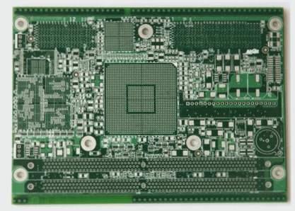
Printed Circuit Board (PCB) Design:
PCBs are vital in electronic product design, connecting components and devices. With advancing technology, PCBs must meet demands for layout, interference resistance, and manufacturability.
Considerations in PCB Design:
- Ensure circuit schematic components match physical objects and network connections.
- Design for power line width, ground wire needs, and impedance matching for high-frequency components.
- Accurately place components for system debugging, ventilation, and heat dissipation.
- Meet manufacturing process requirements for smooth production.