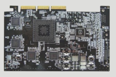
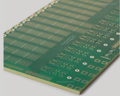
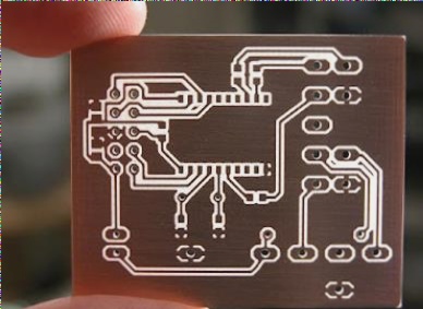
In the process of high-speed printed circuit board (PCB) design, specific principles related to layout and wiring must be carefully adhered to when utilizing PROTEL design software. Practical and proven techniques for high-speed circuit layout and wiring are provided to enhance the reliability and effectiveness of PCB designs. Research findings demonstrate that such designs reduce the product development cycle and bolster market competitiveness.
1. With the increasing complexity and integration of electronic system designs, along with rising clock speeds and device rise times, high-speed circuit design has become a critical aspect of the design process. In high-speed circuit design, the inductance and capacitance on the PCB can cause wires to behave like transmission lines. Improper placement of termination components or incorrect routing of high-speed signals can lead to transmission line effects, resulting in incorrect data output, malfunctioning circuits, or complete operational failure. According to the transmission line model, adverse effects such as signal reflection, crosstalk, electromagnetic interference, and power supply and ground noise can arise in circuit designs. To ensure the reliable operation of high-speed PCBs, designs must meticulously address potential issues during layout and wiring, thereby shortening the product development cycle and enhancing market competitiveness.

2. Layout design of high frequency systems
In PCB board circuit design, layout plays a crucial role, directly impacting wiring efficiency and system reliability. It’s a time-consuming and challenging aspect of overall PCB design. The intricate nature of high-frequency PCBs complicates application of theoretical knowledge to layout design. Therefore, layout designers require extensive experience in high-speed PCB fabrication to navigate design complexities effectively, ensuring circuit reliability and performance. During layout, factors such as mechanical structure, heat dissipation, electromagnetic interference, future wiring convenience, and aesthetics must be comprehensively considered.
Before beginning layout, it’s essential to segment the circuit based on function, separating high-frequency from low-frequency and analog from digital circuits. This separation minimizes transmission delays caused by lengthy traces and enhances capacitor decoupling efficiency. Additionally, careful attention should be paid to component pin orientation to mitigate mutual interference. High-frequency components should be positioned away from chassis and other metal surfaces to reduce parasitic coupling.
Thermal and electromagnetic interactions between components must be managed meticulously during layout, particularly critical in high-frequency systems. Measures such as isolation, heat dissipation, and shielding should be implemented. Components prone to heat, like rectifiers and regulators, require adequate spacing and possibly heat sinks to prevent performance degradation and ensure circuit stability. Moreover, electrolytic capacitors, sensitive to heat, should be positioned away from heat sources to prevent drying of electrolytes, which can compromise performance.
To minimize parasitic coupling, proper guard structures should be incorporated into the layout design. Techniques like vertical plate isolation and minimizing lead length are beneficial. Avoiding connectors and optimizing component placement around noise-sensitive areas such as crystal oscillators and analog signal traces further enhances circuit stability and performance.
Lastly, while ensuring functional integrity, aesthetic considerations should guide overall PCB planning. Components should ideally be aligned parallel or perpendicular to the board surface and edges, promoting ease of installation, welding, and mass production.
3. Wiring of high frequency systems
In high-frequency circuits, parameters like resistance, capacitance, inductance, and mutual inductance of connecting wires significantly influence circuit performance. Effective wiring strategies aim to minimize line resistance, distributed capacitance, and stray inductance to reduce the impact of stray magnetic fields and electromagnetic interference. Utilizing design tools like PROTEL, though common, often focuses solely on layout speed rather than adapting to device characteristic improvements, potentially limiting new device performance.
Special considerations for wiring high-frequency circuits include:
– Minimizing lead bends to reduce external emission of high-frequency signals and mutual interference. Utilize full straight lines where possible, with 45° folds or circular arcs when necessary.
– Shortening lead lengths to optimize signal integrity. PROTEL 99 SE facilitates this through advanced routing techniques.
– Minimizing layer alternations in component connections to reduce use of vias, thereby decreasing distributed capacitance and enhancing signal speed.
– Mitigating cross-interference from parallel signal lines by strategic placement of ground planes and careful routing in adjacent layers.
Implementing these techniques not only improves signal quality but also enhances the overall performance and reliability of high-frequency circuits.
4. Design of power and ground systems
Designing power supply and ground systems for high-frequency circuits necessitates addressing voltage drop and line impedance issues. Two primary solutions include using networked power bus technology or separate power supply layers. While the latter is more complex and costly, networked power bus technology ensures balanced current distribution among components, minimizing voltage drops caused by impedance.
Key considerations for power and ground design include:
– Ensuring low-resistance ground planes for multi-point grounding, crucial for reducing common ground impedance at high frequencies.
– Strategically placing high-frequency decoupling capacitors at chip power and ground terminals to manage transient currents effectively.
– Opting for capacitors with high-frequency characteristics over electrolytic types, which are less effective due to their high distributed inductance.
– Employing impedance matching techniques to prevent signal reflection, crucial for maintaining signal integrity in high-speed digital circuits.
By implementing these strategies, designers can achieve optimal power delivery and ground integrity, critical for reliable high-frequency circuit operation.
5. Other high-speed circuit design technologies
Impedance matching and crosstalk management are pivotal in ensuring signal integrity in high-speed PCB designs. Techniques like parallel AC termination and careful layout planning help minimize signal reflections and electromagnetic interference between adjacent transmission lines.
Designers should also consider differential signal transmission for controlling noise factors in high-speed digital circuits. Differential lines effectively mitigate common-mode noise, ensuring high-speed integration and low power consumption.
6. Conclusion
Advances in electronic technology necessitate a thorough understanding of signal integrity theory to guide and verify high-speed PCB board designs effectively. Implementing the strategies discussed can streamline development cycles, minimize errors, and optimize resource utilization, ensuring the production of high-quality printed circuit boards that meet project budgets and market demands. Continued research and application of new technologies are crucial for designing high-speed PCB boards with superior performance and reliability in competitive market environments.
1. With the increasing complexity and integration of electronic system designs, along with rising clock speeds and device rise times, high-speed circuit design has become a critical aspect of the design process. In high-speed circuit design, the inductance and capacitance on the PCB can cause wires to behave like transmission lines. Improper placement of termination components or incorrect routing of high-speed signals can lead to transmission line effects, resulting in incorrect data output, malfunctioning circuits, or complete operational failure. According to the transmission line model, adverse effects such as signal reflection, crosstalk, electromagnetic interference, and power supply and ground noise can arise in circuit designs. To ensure the reliable operation of high-speed PCBs, designs must meticulously address potential issues during layout and wiring, thereby shortening the product development cycle and enhancing market competitiveness.

2. Layout design of high frequency systems
In PCB board circuit design, layout plays a crucial role, directly impacting wiring efficiency and system reliability. It’s a time-consuming and challenging aspect of overall PCB design. The intricate nature of high-frequency PCBs complicates application of theoretical knowledge to layout design. Therefore, layout designers require extensive experience in high-speed PCB fabrication to navigate design complexities effectively, ensuring circuit reliability and performance. During layout, factors such as mechanical structure, heat dissipation, electromagnetic interference, future wiring convenience, and aesthetics must be comprehensively considered.
Before beginning layout, it’s essential to segment the circuit based on function, separating high-frequency from low-frequency and analog from digital circuits. This separation minimizes transmission delays caused by lengthy traces and enhances capacitor decoupling efficiency. Additionally, careful attention should be paid to component pin orientation to mitigate mutual interference. High-frequency components should be positioned away from chassis and other metal surfaces to reduce parasitic coupling.
Thermal and electromagnetic interactions between components must be managed meticulously during layout, particularly critical in high-frequency systems. Measures such as isolation, heat dissipation, and shielding should be implemented. Components prone to heat, like rectifiers and regulators, require adequate spacing and possibly heat sinks to prevent performance degradation and ensure circuit stability. Moreover, electrolytic capacitors, sensitive to heat, should be positioned away from heat sources to prevent drying of electrolytes, which can compromise performance.
To minimize parasitic coupling, proper guard structures should be incorporated into the layout design. Techniques like vertical plate isolation and minimizing lead length are beneficial. Avoiding connectors and optimizing component placement around noise-sensitive areas such as crystal oscillators and analog signal traces further enhances circuit stability and performance.
Lastly, while ensuring functional integrity, aesthetic considerations should guide overall PCB planning. Components should ideally be aligned parallel or perpendicular to the board surface and edges, promoting ease of installation, welding, and mass production.
3. Wiring of high frequency systems
In high-frequency circuits, parameters like resistance, capacitance, inductance, and mutual inductance of connecting wires significantly influence circuit performance. Effective wiring strategies aim to minimize line resistance, distributed capacitance, and stray inductance to reduce the impact of stray magnetic fields and electromagnetic interference. Utilizing design tools like PROTEL, though common, often focuses solely on layout speed rather than adapting to device characteristic improvements, potentially limiting new device performance.
Special considerations for wiring high-frequency circuits include:
– Minimizing lead bends to reduce external emission of high-frequency signals and mutual interference. Utilize full straight lines where possible, with 45° folds or circular arcs when necessary.
– Shortening lead lengths to optimize signal integrity. PROTEL 99 SE facilitates this through advanced routing techniques.
– Minimizing layer alternations in component connections to reduce use of vias, thereby decreasing distributed capacitance and enhancing signal speed.
– Mitigating cross-interference from parallel signal lines by strategic placement of ground planes and careful routing in adjacent layers.
Implementing these techniques not only improves signal quality but also enhances the overall performance and reliability of high-frequency circuits.
4. Design of power and ground systems
Designing power supply and ground systems for high-frequency circuits necessitates addressing voltage drop and line impedance issues. Two primary solutions include using networked power bus technology or separate power supply layers. While the latter is more complex and costly, networked power bus technology ensures balanced current distribution among components, minimizing voltage drops caused by impedance.
Key considerations for power and ground design include:
– Ensuring low-resistance ground planes for multi-point grounding, crucial for reducing common ground impedance at high frequencies.
– Strategically placing high-frequency decoupling capacitors at chip power and ground terminals to manage transient currents effectively.
– Opting for capacitors with high-frequency characteristics over electrolytic types, which are less effective due to their high distributed inductance.
– Employing impedance matching techniques to prevent signal reflection, crucial for maintaining signal integrity in high-speed digital circuits.
By implementing these strategies, designers can achieve optimal power delivery and ground integrity, critical for reliable high-frequency circuit operation.
5. Other high-speed circuit design technologies
Impedance matching and crosstalk management are pivotal in ensuring signal integrity in high-speed PCB designs. Techniques like parallel AC termination and careful layout planning help minimize signal reflections and electromagnetic interference between adjacent transmission lines.
Designers should also consider differential signal transmission for controlling noise factors in high-speed digital circuits. Differential lines effectively mitigate common-mode noise, ensuring high-speed integration and low power consumption.
6. Conclusion
Advances in electronic technology necessitate a thorough understanding of signal integrity theory to guide and verify high-speed PCB board designs effectively. Implementing the strategies discussed can streamline development cycles, minimize errors, and optimize resource utilization, ensuring the production of high-quality printed circuit boards that meet project budgets and market demands. Continued research and application of new technologies are crucial for designing high-speed PCB boards with superior performance and reliability in competitive market environments.


