Challenges in High-Speed PCB Design and Solutions
- Hardware engineers traditionally rely on experience for PCB design.
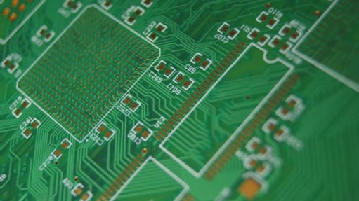
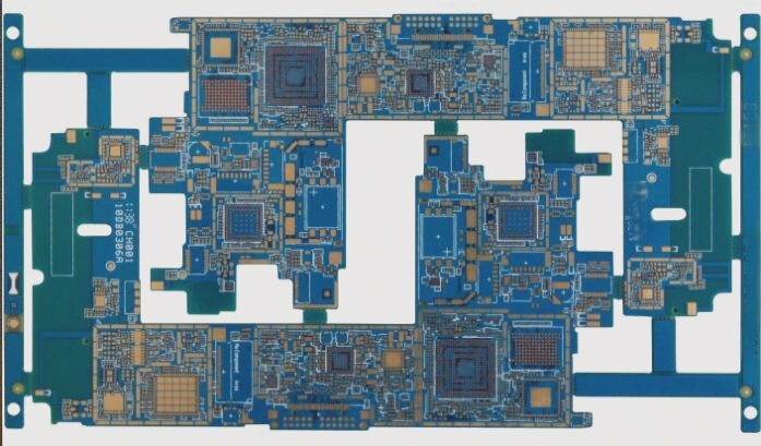
- Signal lines and chip pins buried within PCB layers hinder observation and debugging.
- Difficulty in pinpointing root causes of product failures during testing.
- EMC characteristics evaluation requires measurements in specialized facilities.
- Focus on external radiation in EMC testing may overlook underlying issues.
- Iterative modifications and testing delay time to market.
- Limitations in device models hamper high-speed PCB analysis tools.
- Insufficient IBIS models for signal integrity simulations.
- Lack of SPICE models for effective EMC issue simulation.
Addressing these challenges, engineers can utilize tools like Emscan’s electromagnetic compatibility scanning system. This system employs H-field array probes to detect high-frequency currents on the PCB, providing insights into electromagnetic radiation. By identifying areas with EMI problems early on, engineers can take proactive measures to ensure compliance with electromagnetic compatibility standards.

Understanding the return path of high-frequency signals in multi-layer PCB boards is crucial for managing electromagnetic radiation. While challenges exist in determining signal return paths due to various factors, tools like Emscan offer a solution by visualizing RF currents on the PCB. By leveraging current density maps provided by such systems, engineers can optimize PCB designs and address EMI issues effectively.