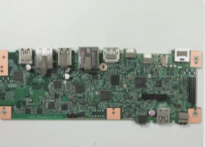
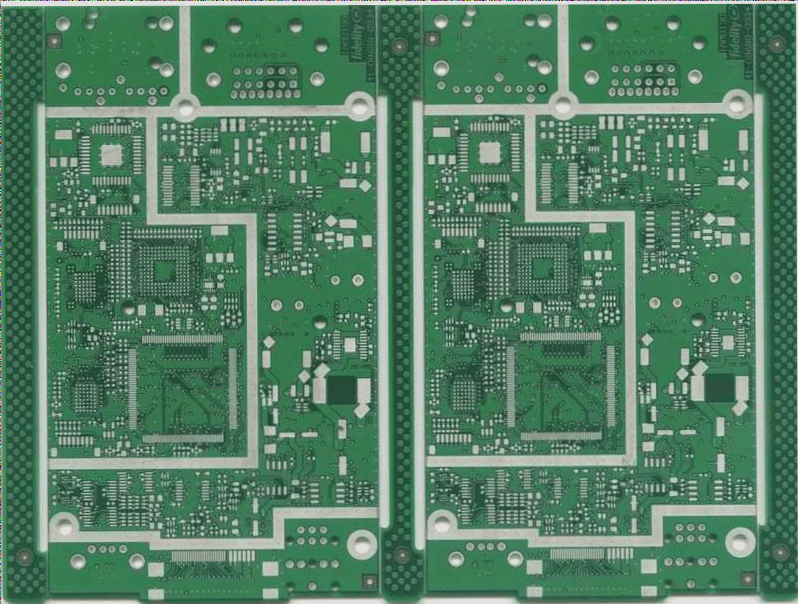
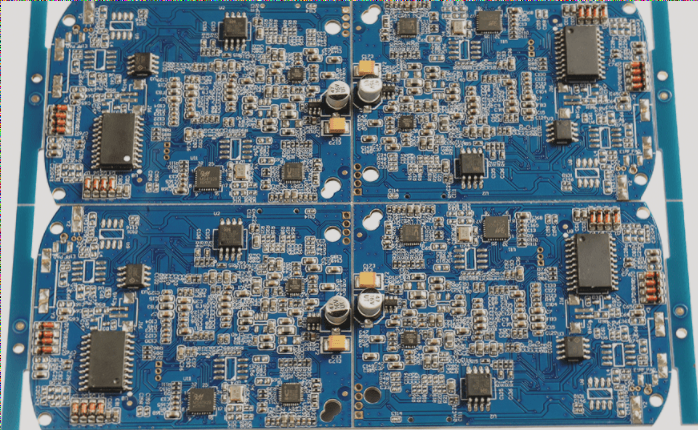
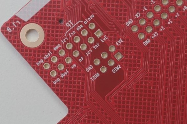
In PCB design, wiring is a crucial step in completing product development. It can be said that all previous preparations lead to this stage. Within the entire PCB, the wiring design process is the most constrained, requiring the least skill yet involving the most extensive workload. PCB wiring encompasses single-sided, double-sided, and multilayer configurations.
There are two approaches to wiring: automatic and interactive. Prior to automatic routing, interactive wiring can be used to pre-route critical lines. It’s important to keep the edges of the input and output ends from being parallel to each other to avoid reflection interference. If necessary, ground wires should be added for isolation, and adjacent layer wiring should be oriented perpendicularly to minimize parasitic coupling.
The effectiveness of automatic routing hinges on a solid layout. Routing rules can be predefined, addressing factors such as the number of bends, vias, and steps. Typically, the process begins with exploring warp wiring, connecting short wires quickly, followed by labyrinth wiring. Initially, optimize the global wiring path and disconnect laid wires as needed, aiming to re-route for enhanced overall performance.
With the current trends in high-density PCB design, through-holes are often deemed unsuitable, consuming valuable routing channels. To address this issue, blind and buried hole technologies have emerged, fulfilling the functions of through-holes while conserving wiring channels, thereby streamlining the wiring process. The PCB design process is both complex and straightforward; mastering it requires extensive experience in electronic engineering design, as true understanding comes through hands-on experience.
1. Management of power supply and ground wire.

Even if the wiring on the entire PCB is executed flawlessly, interference from inadequate power supply and ground wire considerations can diminish product performance, sometimes impacting its success rate. Thus, it is essential to prioritize the wiring of power and ground lines while minimizing noise interference to ensure product quality.
Every engineer involved in electronic product design is aware of the noise generated between ground and power wires. Here are some methods to reduce noise suppression:
(1) It is well-known to place decoupling capacitors between the power supply and ground.
(2) Maximize the width of power and ground wires, ideally with the ground wire being wider than the power wire. The hierarchy should be: ground wire > power wire > signal wire, with typical signal wire widths ranging from 0.2 to 0.3 mm and a minimum of 0.05 to 0.07 mm; power wires should be between 1.2 and 2.5 mm. For digital circuit PCBs, wide ground wires can create loops, forming a ground net (this method should not be used for analog circuits).
(3) Utilize a large copper area as the ground wire, connecting unused spaces on the PCB to the ground. Alternatively, a multi-layer board can be designed, with separate layers for power supply and ground.
2. Common Ground Management for Digital and Analog Circuits
Many PCBs integrate both digital and analog circuits, necessitating careful consideration of mutual interference, particularly noise on the ground wire. Digital circuits operate at high frequencies, while analog circuits are highly sensitive. Signal lines should be distanced from sensitive analog devices, and the PCB should maintain a single node to the external world. Within the PCB, digital and analog grounds should remain separate, only connecting at a single point at the interface (such as connectors). Non-common grounds may also be present, as dictated by system design.
3. Routing Signal Lines on the Power (Ground) Layer
In multi-layer PCBs, limited signal lines may remain in the designated layers, leading to unnecessary layers and increased costs. To address this, consider routing on the power (ground) layer, prioritizing the power layer first, followed by the ground layer to preserve the integrity of the layout.
4. Connecting Pins in Large Area Conductors
In extensive ground (power) areas, the connection of component pins must be comprehensively managed. For optimal electrical performance, component pads should connect directly to the copper surface. However, assembly challenges, such as:
(1) The need for high-power soldering equipment.
(2) Risks of cold solder joints.
To mitigate these, use cross-patterned pads, known as thermal pads, to reduce the likelihood of cold solder joints due to excessive heat during soldering. This same principle applies to multilayer board power (ground) pins.
5. The Role of the Grid System in Wiring
In various CAD systems, routing is often determined by the grid system. A very dense grid can complicate routing and demand more storage and processing power. Some paths become invalid due to component pads or mounting holes. Conversely, a sparse grid negatively impacts distribution efficiency. Therefore, a well-spaced grid system is essential for effective wiring.
The standard distance between component legs is 0.1 inches (2.54 mm), setting the grid system’s basis to 0.1 inches or its integral multiples, such as 0.05 inches, 0.025 inches, or 0.02 inches.
6. Design Rule Check (DRC)
After completing the wiring design, it’s crucial to verify adherence to designer-established rules and ensure they meet PCB production requirements. Key inspection aspects include:
(1) Ensuring reasonable distances between lines, component pads, and holes.
(2) Checking the appropriateness of power and ground wire widths, and assessing tight coupling (low wave impedance). Can any ground areas be widened on the PCB?
(3) Ensuring optimal conditions for critical signal lines, such as minimizing length, adding protection lines, and clearly separating input and output lines.
(4) Verifying the presence of separate grounds for analog and digital circuits.
(5) Checking whether added graphics (such as icons and labels) might cause signal short circuits.
(6) Modifying any unsatisfactory linear shapes.
(7) Ensuring there are process lines on the PCB, with solder mask requirements met and appropriate sizes, ensuring device pad logos do not compromise electrical quality.
(8) Verifying the outer frame of the power ground layer in multilayer boards is not overly reduced, as exposed copper foil can lead to short circuits.
There are two approaches to wiring: automatic and interactive. Prior to automatic routing, interactive wiring can be used to pre-route critical lines. It’s important to keep the edges of the input and output ends from being parallel to each other to avoid reflection interference. If necessary, ground wires should be added for isolation, and adjacent layer wiring should be oriented perpendicularly to minimize parasitic coupling.
The effectiveness of automatic routing hinges on a solid layout. Routing rules can be predefined, addressing factors such as the number of bends, vias, and steps. Typically, the process begins with exploring warp wiring, connecting short wires quickly, followed by labyrinth wiring. Initially, optimize the global wiring path and disconnect laid wires as needed, aiming to re-route for enhanced overall performance.
With the current trends in high-density PCB design, through-holes are often deemed unsuitable, consuming valuable routing channels. To address this issue, blind and buried hole technologies have emerged, fulfilling the functions of through-holes while conserving wiring channels, thereby streamlining the wiring process. The PCB design process is both complex and straightforward; mastering it requires extensive experience in electronic engineering design, as true understanding comes through hands-on experience.
1. Management of power supply and ground wire.
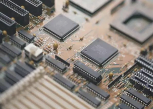
Even if the wiring on the entire PCB is executed flawlessly, interference from inadequate power supply and ground wire considerations can diminish product performance, sometimes impacting its success rate. Thus, it is essential to prioritize the wiring of power and ground lines while minimizing noise interference to ensure product quality.
Every engineer involved in electronic product design is aware of the noise generated between ground and power wires. Here are some methods to reduce noise suppression:
(1) It is well-known to place decoupling capacitors between the power supply and ground.
(2) Maximize the width of power and ground wires, ideally with the ground wire being wider than the power wire. The hierarchy should be: ground wire > power wire > signal wire, with typical signal wire widths ranging from 0.2 to 0.3 mm and a minimum of 0.05 to 0.07 mm; power wires should be between 1.2 and 2.5 mm. For digital circuit PCBs, wide ground wires can create loops, forming a ground net (this method should not be used for analog circuits).
(3) Utilize a large copper area as the ground wire, connecting unused spaces on the PCB to the ground. Alternatively, a multi-layer board can be designed, with separate layers for power supply and ground.
2. Common Ground Management for Digital and Analog Circuits
Many PCBs integrate both digital and analog circuits, necessitating careful consideration of mutual interference, particularly noise on the ground wire. Digital circuits operate at high frequencies, while analog circuits are highly sensitive. Signal lines should be distanced from sensitive analog devices, and the PCB should maintain a single node to the external world. Within the PCB, digital and analog grounds should remain separate, only connecting at a single point at the interface (such as connectors). Non-common grounds may also be present, as dictated by system design.
3. Routing Signal Lines on the Power (Ground) Layer
In multi-layer PCBs, limited signal lines may remain in the designated layers, leading to unnecessary layers and increased costs. To address this, consider routing on the power (ground) layer, prioritizing the power layer first, followed by the ground layer to preserve the integrity of the layout.
4. Connecting Pins in Large Area Conductors
In extensive ground (power) areas, the connection of component pins must be comprehensively managed. For optimal electrical performance, component pads should connect directly to the copper surface. However, assembly challenges, such as:
(1) The need for high-power soldering equipment.
(2) Risks of cold solder joints.
To mitigate these, use cross-patterned pads, known as thermal pads, to reduce the likelihood of cold solder joints due to excessive heat during soldering. This same principle applies to multilayer board power (ground) pins.
5. The Role of the Grid System in Wiring
In various CAD systems, routing is often determined by the grid system. A very dense grid can complicate routing and demand more storage and processing power. Some paths become invalid due to component pads or mounting holes. Conversely, a sparse grid negatively impacts distribution efficiency. Therefore, a well-spaced grid system is essential for effective wiring.
The standard distance between component legs is 0.1 inches (2.54 mm), setting the grid system’s basis to 0.1 inches or its integral multiples, such as 0.05 inches, 0.025 inches, or 0.02 inches.
6. Design Rule Check (DRC)
After completing the wiring design, it’s crucial to verify adherence to designer-established rules and ensure they meet PCB production requirements. Key inspection aspects include:
(1) Ensuring reasonable distances between lines, component pads, and holes.
(2) Checking the appropriateness of power and ground wire widths, and assessing tight coupling (low wave impedance). Can any ground areas be widened on the PCB?
(3) Ensuring optimal conditions for critical signal lines, such as minimizing length, adding protection lines, and clearly separating input and output lines.
(4) Verifying the presence of separate grounds for analog and digital circuits.
(5) Checking whether added graphics (such as icons and labels) might cause signal short circuits.
(6) Modifying any unsatisfactory linear shapes.
(7) Ensuring there are process lines on the PCB, with solder mask requirements met and appropriate sizes, ensuring device pad logos do not compromise electrical quality.
(8) Verifying the outer frame of the power ground layer in multilayer boards is not overly reduced, as exposed copper foil can lead to short circuits.

