High-Speed PCB Circuit Board Design Considerations
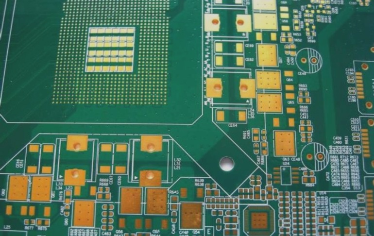
- When coating blank areas of signal layers with copper in high-speed PCB design, it is crucial to consider how the copper coating should be distributed between grounding and power supply.
Copper Coating Distribution:
- Primarily ground copper plating in blank areas near high-speed signal lines while maintaining a sufficient distance to avoid affecting trace impedance.
- Consider using the microstrip line model for characteristic impedance calculations on power planes and the stripline model for signal lines between power supply and ground planes.
- When adding test points on high-density PCBs, ensure alignment with test equipment requirements as manual addition may be necessary for strict specifications.
Effects of Adding Test Points:
- Adding test points can impact high-speed signals depending on method and signal speed, with simulation recommended to assess the magnitude of impact.
- Proper ground connections between PCBs in a system are essential to minimize impedance and reduce noise, especially at interfaces where power or signals are exchanged.
- For high-speed PCB design resources, consider foreign technical books and data that address the increasing demands for high-speed, high-density wiring in communication networks and computing devices.
Characteristic Impedance Formulas:
- Microstrip: Z = {87 / [sqrt(Er + 1.41)]} ln[5.98H / (0.8W + T)]
- Stripline: Z = [60 / sqrt(Er)] ln{4H / [0.67π(T + 0.8W)]}
By following these guidelines and understanding the impact of copper distribution, test points, ground connections, and characteristic impedance formulas, high-speed PCB designs can effectively meet the demands of modern communication networks and computing devices.
Common Questions About PCB Design
-
Can a ground wire be added to a differential signal line?
Typically, it is not recommended to add a ground wire in the middle of a differential signal line. Differential signals offer advantages such as flux cancellation and noise immunity through their coupling benefits. Introducing a ground wire can disrupt this coupling effect.
-
Does rigid-flex board design require special software and specifications?
Rigid-flex board design can be achieved using general PCB design software for flexible printed circuit (FPC) design, usually in Gerber format. Different FPC manufacturers have specific requirements for minimum line widths, spacing, and apertures due to varying manufacturing processes. Copper reinforcement at flexible circuit board turn points is also an option. For circuit board processing in China, search online using the keyword “FPC” for relevant results.
-
What is the principle for selecting grounding points between the PCB and the case?
The principle involves utilizing chassis ground to establish a low-impedance path for returning current and controlling its flow. Connecting the PCB ground to the chassis ground near high-frequency devices or clock generators with fixing screws helps minimize the current loop area and decrease electromagnetic radiation.