High-Frequency PCB Design Tips for Optimal Interconnections
- Ensure transmission line corners are at a 45° angle to reduce return loss.
- Use high-performance insulated circuit boards with precise insulation constant values to manage electromagnetic fields effectively.
- Enhance PCB design specifications for high-precision etching to address issues related to microwave frequency.
- Avoid components with protruding leads in high-frequency environments; opt for surface mount components instead.
- Avoid via processing on signal vias in sensitive boards to prevent lead inductance.
- Choose electroless nickel plating or immersion gold plating processes for better skin effect at high frequencies.
- Consider using a solder dam instead of covering the entire board surface with solder mask material to maintain electromagnetic energy balance.
Implementing these techniques in high-frequency PCB design can optimize your interconnection layout. Remember, a back-side copper-clad coplanar microstrip design may offer a more cost-effective solution compared to a stripline design.
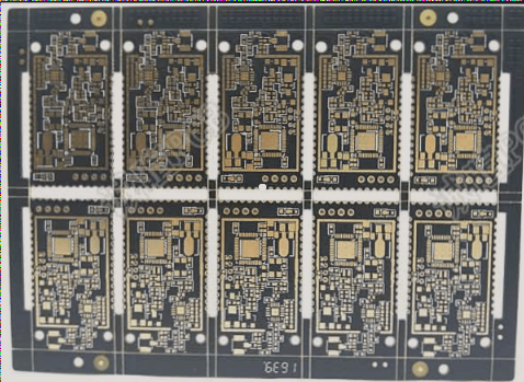
About WellCircuits Limited
WellCircuits Limited specializes in manufacturing high-precision double-sided, multilayer, and impedance-controlled circuit boards. Our product range includes boards with blind buried vias, thick copper, HDI, backplanes, and rigid-flex combinations, catering to diverse customer requirements such as buried capacitance and resistance, Golden Finger, and more.