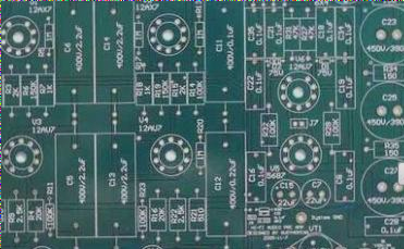
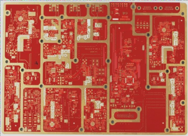
**Double-sided PCB Manufacturing Process**
In recent years, the common methods for producing double-sided metallized PCBs are the SMOBC (Solder Mask Over Bare Copper) method and the pattern plating method. In some instances, process conductors are also utilized.
1. **Graphic Electroplating Process:**
Foil board – blanking – drilling front edge hole – CNC drilling – inspection – deburring – electroless thin copper plating – thin copper electroplating – inspection – brushing – film (or screen printing) – exposure and development (or curing) – inspection – board repair – graphic plating (Cu(Sn/Pb)) – film removal – etching – testing and board repair – nickel-plated plug – hot melt cleaning – electrical continuity detection – cleaning treatment – mesh seal resistance welding pattern – curing – screen printing symbol – curing – shaping – cleaning and drying – inspection – packaging – finished product.

1. **In this method, both “electroless copper plating” and “electroless copper plating” processes can be replaced by a single “electroless copper plating” process, each having its own advantages and disadvantages. The pattern plating-etching method for double-sided metallization was a typical process used in the 1960s and 1970s. In the 1980s, the development of bare copper-coated solder film (SMOBC) gained traction, especially in precision double-sided panel manufacturing, and gradually became the mainstream process.**
2. **SMOBC Process:**
The primary advantage of the SMOBC board is that it resolves issues like short circuits caused by solder bridges between thin traces. Furthermore, with a consistent lead-to-tin ratio, it offers better solderability and storage stability compared to hot air leveled boards. There are various methods for manufacturing SMOBC boards, including the standard pattern plating method, which subtracts lead-tin from the back, and alternatives like using tin-plated or immersion tin instead of electroplated lead-tin. Other methods include the pattern plating process for SMOBC with hole plating, hole plugging, or mask hole techniques, as well as the additive SMOBC process.
The following focuses mainly on the SMOBC pattern plating method, the lead-tin stripping process, and the SMOBC process involving the hole plugging technique.
1. **Pattern Electroplating Method and Lead-Tin Stripping Process:**
The SMOBC process using pattern plating and subsequent lead-tin re-deposition closely resembles the conventional pattern plating process, with changes made only after etching.
For a double-sided copper foil board, the process begins with pattern plating followed by etching, lead-tin removal, inspection, cleaning, and the application of soldering graphics. Then, nickel plating is applied to plugged holes, followed by the application of hot air leveling, further cleaning, grid marking, shape processing, final cleaning, and drying. The final steps include product inspection, packaging, and labeling.
2. **Main Steps of the Hole Plugging Method:**
The process using the hole plugging method for double-sided aluminum foil boards involves drilling, electroless copper plating, and full board copper plating. The holes are then plugged, and the reticulated imaging (positive image) is applied, followed by etching. After etching, the mesh material is removed, and the plugging material is cleaned. The board is then subjected to soldering, nickel plating, gold plating, tape application, hot air leveling, and final processing before inspection and packaging.
This PCB production process is relatively straightforward, with the key step being the use of ink for hole plugging and cleaning.
If hole-blocking ink is not used during the hole plugging and grid imaging steps, a special masking dry film can be applied to cover the holes. This film is then exposed to create a negative image. This method eliminates the issue of cleaning ink out of the holes, but it places higher demands on the dry film coverage quality.
The SMOBC process is based on the production of a metallized bare copper double-sided board, followed by the application of the hot air leveling process.
If your have any questions about PCB ,please contact me info@wellcircuits.com
In recent years, the common methods for producing double-sided metallized PCBs are the SMOBC (Solder Mask Over Bare Copper) method and the pattern plating method. In some instances, process conductors are also utilized.
1. **Graphic Electroplating Process:**
Foil board – blanking – drilling front edge hole – CNC drilling – inspection – deburring – electroless thin copper plating – thin copper electroplating – inspection – brushing – film (or screen printing) – exposure and development (or curing) – inspection – board repair – graphic plating (Cu(Sn/Pb)) – film removal – etching – testing and board repair – nickel-plated plug – hot melt cleaning – electrical continuity detection – cleaning treatment – mesh seal resistance welding pattern – curing – screen printing symbol – curing – shaping – cleaning and drying – inspection – packaging – finished product.

1. **In this method, both “electroless copper plating” and “electroless copper plating” processes can be replaced by a single “electroless copper plating” process, each having its own advantages and disadvantages. The pattern plating-etching method for double-sided metallization was a typical process used in the 1960s and 1970s. In the 1980s, the development of bare copper-coated solder film (SMOBC) gained traction, especially in precision double-sided panel manufacturing, and gradually became the mainstream process.**
2. **SMOBC Process:**
The primary advantage of the SMOBC board is that it resolves issues like short circuits caused by solder bridges between thin traces. Furthermore, with a consistent lead-to-tin ratio, it offers better solderability and storage stability compared to hot air leveled boards. There are various methods for manufacturing SMOBC boards, including the standard pattern plating method, which subtracts lead-tin from the back, and alternatives like using tin-plated or immersion tin instead of electroplated lead-tin. Other methods include the pattern plating process for SMOBC with hole plating, hole plugging, or mask hole techniques, as well as the additive SMOBC process.
The following focuses mainly on the SMOBC pattern plating method, the lead-tin stripping process, and the SMOBC process involving the hole plugging technique.
1. **Pattern Electroplating Method and Lead-Tin Stripping Process:**
The SMOBC process using pattern plating and subsequent lead-tin re-deposition closely resembles the conventional pattern plating process, with changes made only after etching.
For a double-sided copper foil board, the process begins with pattern plating followed by etching, lead-tin removal, inspection, cleaning, and the application of soldering graphics. Then, nickel plating is applied to plugged holes, followed by the application of hot air leveling, further cleaning, grid marking, shape processing, final cleaning, and drying. The final steps include product inspection, packaging, and labeling.
2. **Main Steps of the Hole Plugging Method:**
The process using the hole plugging method for double-sided aluminum foil boards involves drilling, electroless copper plating, and full board copper plating. The holes are then plugged, and the reticulated imaging (positive image) is applied, followed by etching. After etching, the mesh material is removed, and the plugging material is cleaned. The board is then subjected to soldering, nickel plating, gold plating, tape application, hot air leveling, and final processing before inspection and packaging.
This PCB production process is relatively straightforward, with the key step being the use of ink for hole plugging and cleaning.
If hole-blocking ink is not used during the hole plugging and grid imaging steps, a special masking dry film can be applied to cover the holes. This film is then exposed to create a negative image. This method eliminates the issue of cleaning ink out of the holes, but it places higher demands on the dry film coverage quality.
The SMOBC process is based on the production of a metallized bare copper double-sided board, followed by the application of the hot air leveling process.
If your have any questions about PCB ,please contact me info@wellcircuits.com


