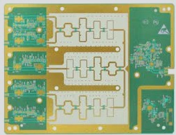
1. PCB vias are holes on printed circuit boards used to create electrical connections between different layers of the PCB, facilitate the installation of PTH components, or connect to external components such as screws and connectors.
2. Generally speaking, PCB vias fall into three main categories: through holes, blind holes, and buried holes.

**PCB Vias Types**
Through hole, blind hole, buried hole, micro hole, through hole in solder pad.
1. **Through Hole**
Through holes are the most common type of vias in PCBs. They are created by drilling a hole through the PCB and then filling it with conductive materials such as copper. Through holes are typically used to connect components to other layers of the PCB and provide structural support. They are drilled from the top layer to the bottom layer of the PCB. When viewing the bare PCB with sunlight, the through hole allows light to pass through.
2. **Blind Hole**
Blind holes are similar to through holes but only extend partially through the PCB, connecting the outer copper layer to internal layers without penetrating through the entire board. Blind holes are ideal for multi-layer PCBs with space constraints.
3. **Buried Hole**
Buried holes are entirely enclosed within the PCB layers, connecting two or more internal copper layers. They are especially suited for high-density PCBs where space is limited.
4. **Micro Through-Hole**
Micro through-holes are very small vias used in high-density PCBs with limited space. These vias generally have a maximum diameter of 0.15 millimeters, an aspect ratio of up to 1:1, and a maximum depth of 0.25 millimeters. Micro vias are well-suited for high-speed signals and are commonly used in mobile phones and other compact electronic devices.
5. **Through Holes in Solder Pad**
Through holes in solder pads are placed within the solder pads of external components. The advantages of using through holes in pads include:
1) Expansion of signal paths, which mitigates the effects of inductance and capacitance.
2) Reduction in PCB size and accommodation for small grounding areas.
These vias are particularly suitable for BGA components. Note that back drilling is often required to eliminate signal echoes in the remaining part of the through hole.
**Design of PCB Through Holes**
1. For simple circuits, vias may not be necessary. However, in multi-layer PCBs, the inclusion of vias is often essential.
2. In multi-layer boards, vias can increase component density by enabling vertical connections between layers.
3. As the number of PCB layers increases, wiring density also rises. Through holes connect different layers and facilitate vertical connectivity.
4. Without vias, wiring can become challenging, particularly with densely packed components such as BGAs, connectors, and multi-layer designs.
5. Vias enhance the transmission of interlayer signals and power. Without them, all components would be confined to the same plane, making it difficult to route surface-mounted components in multi-layer PCBs.
Electroplating via filling offers several benefits:
– It supports the design of stacked holes and holes in discs.
– Enhances electrical performance, especially for high-frequency applications.
– Aids in heat dissipation.
– Combines plugging and electrical interconnections in a single step.
– Electroplated copper in blind holes provides higher reliability and better conductivity compared to conductive adhesives.


