1. A circuit diagram, also known as a PCB schematic, is a graphical representation of the components required to create a circuit board.
2. The schematic also indicates the location of these components on the circuit board, as well as all other aspects of the circuit design that connect the circuit board.

Circuit diagram
A circuit diagram is a schematic layout diagram that represents the composition and relationship of various components using standardized physical and electrical symbols for research and engineering planning purposes. It uses circuit component symbols to represent circuit connections and provides a planning solution for analyzing performance, and installing electronic and electrical products. Engineers can leisurely perform circuit design on paper or computer and confirm its completeness before actual installation, improving and fixing errors through debugging until successful.
Composition of circuit diagram
The circuit diagram mainly consists of four parts: component symbols, wiring, nodes, and annotations.
1. The component symbol represents the component in the actual circuit and its shape is not necessarily similar to the actual component but generally represents the characteristics of the component. It also represents the number of pins consistent with the actual component.
2. Wiring represents the actual wires in a circuit. In the schematic, it is often represented as a single wire, but in reality, it can be various shapes of copper foil blocks in commonly used printed circuit boards.
3. Nodes represent the connection relationship between several component pins or wires. All component pins and wires connected to nodes are conductive.
4. Annotations are important in circuit diagrams and all text in the circuit diagram can be classified as annotations. They are used to indicate the model, name, and other information about the components.
How to convert a circuit diagram to PCB?
1. Design a schematic diagram according to the project’s requirements, including the routing of the circuit and which electronic components to use.
2. Use circuit diagram software, such as Protel or PADS, to draw PCB boards according to the schematic diagram. The drawing board involves packaging and arranging components and connecting them online.
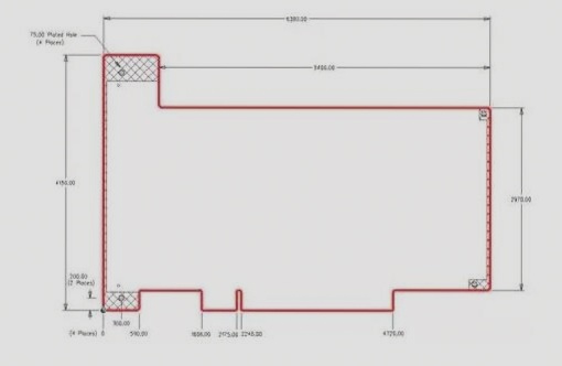
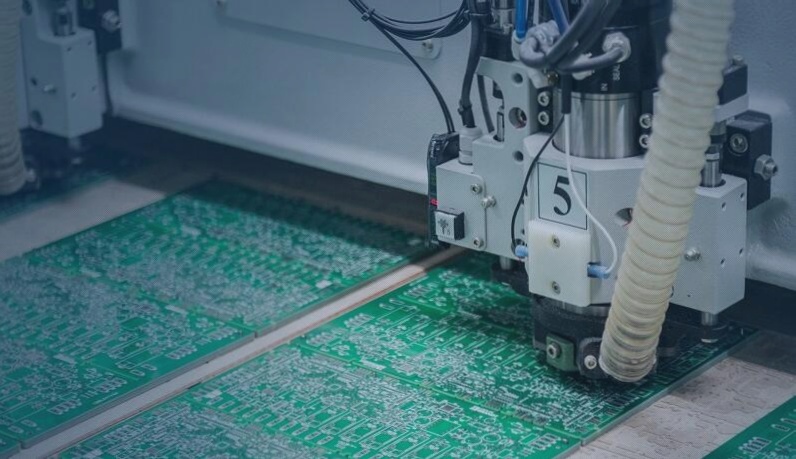
3. Provide the drawings to the PCB manufacturer for the cutting of a large piece of board into small pieces that meet the requirements based on the size of the circuit board.
4. Perform punching for screw holes, fixed installation holes, etc.
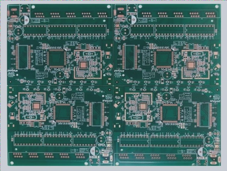
5. After copper deposition, electroplating, film removal, etching, green oil, and other processes, a PCB board can be obtained.
It is theoretically possible to correspond the circuit diagram to the components on the PCB board, but the difficulty mainly depends on factors such as component type, component quantity, and PCB board layout. For PCB boards with complex circuits, it is best to combine relevant information and analyze them comprehensively. Additionally, there are many automated circuit analysis software on the market that can generate corresponding schematic diagrams by scanning PCB boards, achieving faster and more accurate conversion between PCB boards and schematic diagrams.
Using circuit diagram simulation software for circuit-aided design and virtual circuit experiments can improve engineers’ work efficiency, save learning time, and make physical diagrams more intuitive.
2. The schematic also indicates the location of these components on the circuit board, as well as all other aspects of the circuit design that connect the circuit board.

Circuit diagram
A circuit diagram is a schematic layout diagram that represents the composition and relationship of various components using standardized physical and electrical symbols for research and engineering planning purposes. It uses circuit component symbols to represent circuit connections and provides a planning solution for analyzing performance, and installing electronic and electrical products. Engineers can leisurely perform circuit design on paper or computer and confirm its completeness before actual installation, improving and fixing errors through debugging until successful.
Composition of circuit diagram
The circuit diagram mainly consists of four parts: component symbols, wiring, nodes, and annotations.
1. The component symbol represents the component in the actual circuit and its shape is not necessarily similar to the actual component but generally represents the characteristics of the component. It also represents the number of pins consistent with the actual component.
2. Wiring represents the actual wires in a circuit. In the schematic, it is often represented as a single wire, but in reality, it can be various shapes of copper foil blocks in commonly used printed circuit boards.
3. Nodes represent the connection relationship between several component pins or wires. All component pins and wires connected to nodes are conductive.
4. Annotations are important in circuit diagrams and all text in the circuit diagram can be classified as annotations. They are used to indicate the model, name, and other information about the components.
How to convert a circuit diagram to PCB?
1. Design a schematic diagram according to the project’s requirements, including the routing of the circuit and which electronic components to use.
2. Use circuit diagram software, such as Protel or PADS, to draw PCB boards according to the schematic diagram. The drawing board involves packaging and arranging components and connecting them online.
3. Provide the drawings to the PCB manufacturer for the cutting of a large piece of board into small pieces that meet the requirements based on the size of the circuit board.
4. Perform punching for screw holes, fixed installation holes, etc.
5. After copper deposition, electroplating, film removal, etching, green oil, and other processes, a PCB board can be obtained.
It is theoretically possible to correspond the circuit diagram to the components on the PCB board, but the difficulty mainly depends on factors such as component type, component quantity, and PCB board layout. For PCB boards with complex circuits, it is best to combine relevant information and analyze them comprehensively. Additionally, there are many automated circuit analysis software on the market that can generate corresponding schematic diagrams by scanning PCB boards, achieving faster and more accurate conversion between PCB boards and schematic diagrams.
Using circuit diagram simulation software for circuit-aided design and virtual circuit experiments can improve engineers’ work efficiency, save learning time, and make physical diagrams more intuitive.


