The Evolution of PCB Technology and Identifying PCB Layers
With the rapid advancement of integrated circuit technology, circuit boards have transitioned from single-layer to multi-layer designs, posing challenges in identifying the number of PCB layers accurately.
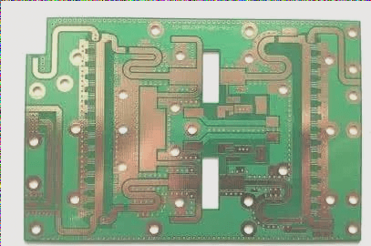
Composition of Circuit Boards
The substrate of a circuit board consists of insulating, heat-resistant materials with visible circuitry made of copper foil. Etching away portions of copper foil during manufacturing creates a network of small circuits, known as traces or wiring, facilitating electrical connections.
Importance of Solder Mask
Circuit boards are typically green or brown due to the solder mask, an insulating protective layer safeguarding copper traces and preventing improper soldering. Multilayer boards, commonly used in motherboards and graphics cards, enhance wiring area by incorporating multiple single or double-sided boards with insulating layers.

Identifying the Number of PCB Layers
The number of layers in a PCB indicates the independent wiring layers it possesses, with common multi-layer structures ranging from 4 to 8 layers. To determine the number of layers, examining via holes is crucial.
Utilization of Buried and Blind Via Technologies
Multi-layer boards employ buried and blind via technologies for circuit connections. By observing via holes, one can differentiate between 4, 6, 8, or 10-layer PCBs. In 4-layer boards, vias connect specific wiring layers, aiding in layer identification.
Identifying PCB Layers Through Via Holes
Presence of vias on the front but not the back suggests a 6 or 8-layer board, while vias on both sides indicate a 4-layer board. A helpful tip is to hold the board against a light source; light passing through via holes signifies a higher layer count.