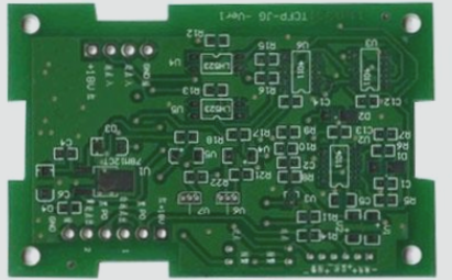
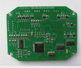
In PCB design and layout, the performance of a stepper motor drive board often falls short of the specifications outlined in the documentation. While the board may function, issues such as current loss, insufficient speed, and poor waveform quality arise. Through in-depth analysis, it becomes evident that certain fundamental PCB wiring principles were overlooked. Upon modification, performance significantly improves, underscoring the critical nature of proper PCB wiring, especially in high-power supplies and sensors that demand stringent wiring standards.
PCB wiring serves to establish pathways for power signals to connect various devices, much like building roads that link cities for vehicles.
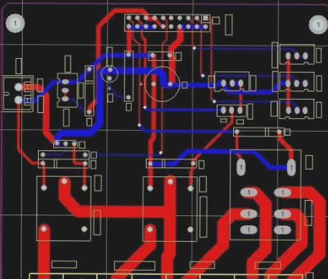
In PCB layout and design, particularly with switching power supplies, high-frequency signals are involved. Any printed trace can act as an antenna; its length and width impact impedance and inductance, thereby influencing frequency response. Even traces carrying DC signals can inadvertently couple with nearby radio frequency signals, potentially causing circuit issues and radiation of interference. Consequently, traces carrying AC current should be kept as short and wide as possible, requiring components connected to these traces to be placed in close proximity. The length of a printed trace is directly proportional to its inductance and impedance, while the width has an inverse relationship. Longer traces can transmit and receive lower frequencies, radiating more radio frequency energy. To minimize loop resistance, increase the width of power traces in accordance with the current levels on the PCB. Additionally, align power and ground traces with the direction of the current to enhance noise immunity. Grounding is crucial in the four current loops of a switching power supply, acting as a common reference point and a key method for controlling interference. Careful placement of grounding wires in the layout is essential, as mixing various grounds can lead to instability in power supply operation.
When designing ground wires, consider these points:
1. Opt for single-point grounding. The common terminal of the filter capacitor should serve as the sole connection point for other grounding points coupling to the high-current AC ground. This connection should be aligned with the grounding point of this level, addressing changes in current return paths and the impedance of the line, which can affect ground potential and introduce interference. In a switching power supply, the wiring and inductance between devices have a minor effect, while circulating currents from the grounding circuit significantly influence interference. Connect the ground pin to the ground wires of multiple devices in the rectifier’s current loop, linking them to the corresponding filter capacitors’ ground pins to stabilize power supply operation and prevent self-excitation. If a single point is impractical, use a common ground, connecting two diodes or a small resistor at that location to a concentrated area of copper foil.

2. Use the thickest possible ground wire. If the ground wire is too thin, the ground potential may fluctuate with current changes, leading to instability in the timing signal levels of electronic equipment and reduced noise immunity. Therefore, ensure that each high-current ground terminal employs printed traces that are both short and wide. It’s advisable to increase the width of both power and ground traces as much as possible, ideally making the ground trace wider than the power trace. The hierarchy should be: ground trace > power trace > signal trace. If feasible, the ground trace width should exceed 3mm, and a large copper area can also serve as a ground connection. Utilize unused spaces on the printed circuit board as additional ground areas. When performing global routing, the following principles should also be adhered to:
(1) PCB routing direction: From the perspective of the soldering surface, the component layout should align as closely as possible with the schematic diagram. The routing direction is best aligned with the circuit diagram’s layout, as various operations on the soldering surface may be necessary during production. This alignment facilitates inspection, debugging, and parameter verification throughout the manufacturing process (note: this pertains to meeting circuit performance standards and the overall installation and panel layout requirements).
PCB wiring serves to establish pathways for power signals to connect various devices, much like building roads that link cities for vehicles.
In PCB layout and design, particularly with switching power supplies, high-frequency signals are involved. Any printed trace can act as an antenna; its length and width impact impedance and inductance, thereby influencing frequency response. Even traces carrying DC signals can inadvertently couple with nearby radio frequency signals, potentially causing circuit issues and radiation of interference. Consequently, traces carrying AC current should be kept as short and wide as possible, requiring components connected to these traces to be placed in close proximity. The length of a printed trace is directly proportional to its inductance and impedance, while the width has an inverse relationship. Longer traces can transmit and receive lower frequencies, radiating more radio frequency energy. To minimize loop resistance, increase the width of power traces in accordance with the current levels on the PCB. Additionally, align power and ground traces with the direction of the current to enhance noise immunity. Grounding is crucial in the four current loops of a switching power supply, acting as a common reference point and a key method for controlling interference. Careful placement of grounding wires in the layout is essential, as mixing various grounds can lead to instability in power supply operation.
When designing ground wires, consider these points:
1. Opt for single-point grounding. The common terminal of the filter capacitor should serve as the sole connection point for other grounding points coupling to the high-current AC ground. This connection should be aligned with the grounding point of this level, addressing changes in current return paths and the impedance of the line, which can affect ground potential and introduce interference. In a switching power supply, the wiring and inductance between devices have a minor effect, while circulating currents from the grounding circuit significantly influence interference. Connect the ground pin to the ground wires of multiple devices in the rectifier’s current loop, linking them to the corresponding filter capacitors’ ground pins to stabilize power supply operation and prevent self-excitation. If a single point is impractical, use a common ground, connecting two diodes or a small resistor at that location to a concentrated area of copper foil.

2. Use the thickest possible ground wire. If the ground wire is too thin, the ground potential may fluctuate with current changes, leading to instability in the timing signal levels of electronic equipment and reduced noise immunity. Therefore, ensure that each high-current ground terminal employs printed traces that are both short and wide. It’s advisable to increase the width of both power and ground traces as much as possible, ideally making the ground trace wider than the power trace. The hierarchy should be: ground trace > power trace > signal trace. If feasible, the ground trace width should exceed 3mm, and a large copper area can also serve as a ground connection. Utilize unused spaces on the printed circuit board as additional ground areas. When performing global routing, the following principles should also be adhered to:
(1) PCB routing direction: From the perspective of the soldering surface, the component layout should align as closely as possible with the schematic diagram. The routing direction is best aligned with the circuit diagram’s layout, as various operations on the soldering surface may be necessary during production. This alignment facilitates inspection, debugging, and parameter verification throughout the manufacturing process (note: this pertains to meeting circuit performance standards and the overall installation and panel layout requirements).


