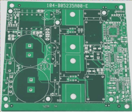
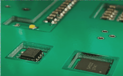
When processing PCBA, a pre-production meeting must be conducted first, and the electronic components supplied for PCBA must be purchased and inspected. A dedicated PCBA incoming inspection station should be established to rigorously check the following items to ensure that the components are free from defects. This approach is essential for guaranteeing quality and minimizing rework and repair efforts. I will elaborate on the relevant details below.
1. How to control the quality of PCBA processing
1. Holding a pre-production meeting after receiving a PCBA processing order is particularly crucial. This process primarily involves analyzing the PCB Gerber files and submitting manufacturability reports (DFM) tailored to various customer requirements. Many smaller manufacturers often overlook this step. However, neglecting it can lead to quality issues arising from inadequate PCB design, resulting in excessive rework and repairs.

—
2. Purchase and Inspection of Electronic Components for PCBA
The procurement channels for electronic components must be rigorously managed, ensuring that goods are sourced from reputable distributors and original manufacturers to prevent the use of second-hand or counterfeit materials. Additionally, a dedicated PCBA incoming inspection station should be established to meticulously verify the following items, ensuring the components are free from defects.
PCB: Assess the reflow oven’s temperature test, check for any blocked or leaking through holes without flying leads, and ensure the board’s surface is not warped.
IC: Verify that the screen printing matches exactly with the specifications, while maintaining the BOM in a controlled temperature and humidity environment.
3. SMT Assembly
Solder paste printing and reflow oven temperature control systems are critical in the assembly process, requiring high-quality laser templates that meet stringent processing standards. Depending on the PCB requirements, adjustments may be necessary for the steel mesh or U-shaped holes, which should be produced in accordance with the specific process guidelines. Temperature control within the reflow oven is vital for optimal solder paste wetting and mesh adhesion and should follow the standard SOP operation guide. Furthermore, rigorous implementation of AOI testing can significantly minimize defects arising from human error.
4. Plug-in Processing
In the plug-in phase, the design of wave soldering molds is crucial. PE engineers must continually refine their methods and gather insights on mold utilization to enhance productivity.
5. PCBA Processing Board Testing
For orders requiring PCBA testing, the main testing procedures include ICT (In-Circuit Test), FCT (Functional Test), combustion testing (aging test), temperature and humidity testing, and drop testing.
2. Considerations for PCBA Processing
1. The minimum clearance between the copper foil and the board edge must be 0.5mm, the component to board edge should be 5.0mm, and the pad to board edge must be 4.0mm.
2. The minimum spacing between copper foils is 0.3mm for single-sided boards and 0.2mm for double-sided boards. (Designers should note that metal shell components in double-sided boards must contact the PCB during insertion. The top pad should remain closed and sealed with either silk screen ink or solder mask.)
3. Jumpers are prohibited beneath ICs or under large-volume metal casing components, such as potentiometers and motors.
4. Electrolytic capacitors must not come into contact with heating components like transformers, thermistors, high-power resistors, or heat sinks. The minimum distance between the heat sink and the electrolytic capacitor should be 10mm, with a 2.0mm gap for other components.
5. Large components (e.g., transformers, electrolytic capacitors over 15mm in diameter, and high-current sockets) require enlarged pads.
6. The minimum line width is 0.3mm for single-sided boards and 0.2mm for double-sided boards (with the minimum copper foil width also at 1.0mm).
7. There should be no copper foil (except for grounding) or components (unless specified by the structural drawing) within 5mm of the screw hole radius.
8. The pad size (diameter) for general through-hole mounting components should be twice the aperture. The minimum size for double-sided boards is 1.5mm, while for single-sided boards, it is 2.0mm. (If round pads are not applicable, oval pads may be utilized.)
—
Let me know if you need further adjustments!
1. How to control the quality of PCBA processing
1. Holding a pre-production meeting after receiving a PCBA processing order is particularly crucial. This process primarily involves analyzing the PCB Gerber files and submitting manufacturability reports (DFM) tailored to various customer requirements. Many smaller manufacturers often overlook this step. However, neglecting it can lead to quality issues arising from inadequate PCB design, resulting in excessive rework and repairs.

—
2. Purchase and Inspection of Electronic Components for PCBA
The procurement channels for electronic components must be rigorously managed, ensuring that goods are sourced from reputable distributors and original manufacturers to prevent the use of second-hand or counterfeit materials. Additionally, a dedicated PCBA incoming inspection station should be established to meticulously verify the following items, ensuring the components are free from defects.
PCB: Assess the reflow oven’s temperature test, check for any blocked or leaking through holes without flying leads, and ensure the board’s surface is not warped.
IC: Verify that the screen printing matches exactly with the specifications, while maintaining the BOM in a controlled temperature and humidity environment.
3. SMT Assembly
Solder paste printing and reflow oven temperature control systems are critical in the assembly process, requiring high-quality laser templates that meet stringent processing standards. Depending on the PCB requirements, adjustments may be necessary for the steel mesh or U-shaped holes, which should be produced in accordance with the specific process guidelines. Temperature control within the reflow oven is vital for optimal solder paste wetting and mesh adhesion and should follow the standard SOP operation guide. Furthermore, rigorous implementation of AOI testing can significantly minimize defects arising from human error.
4. Plug-in Processing
In the plug-in phase, the design of wave soldering molds is crucial. PE engineers must continually refine their methods and gather insights on mold utilization to enhance productivity.
5. PCBA Processing Board Testing
For orders requiring PCBA testing, the main testing procedures include ICT (In-Circuit Test), FCT (Functional Test), combustion testing (aging test), temperature and humidity testing, and drop testing.
2. Considerations for PCBA Processing
1. The minimum clearance between the copper foil and the board edge must be 0.5mm, the component to board edge should be 5.0mm, and the pad to board edge must be 4.0mm.
2. The minimum spacing between copper foils is 0.3mm for single-sided boards and 0.2mm for double-sided boards. (Designers should note that metal shell components in double-sided boards must contact the PCB during insertion. The top pad should remain closed and sealed with either silk screen ink or solder mask.)
3. Jumpers are prohibited beneath ICs or under large-volume metal casing components, such as potentiometers and motors.
4. Electrolytic capacitors must not come into contact with heating components like transformers, thermistors, high-power resistors, or heat sinks. The minimum distance between the heat sink and the electrolytic capacitor should be 10mm, with a 2.0mm gap for other components.
5. Large components (e.g., transformers, electrolytic capacitors over 15mm in diameter, and high-current sockets) require enlarged pads.
6. The minimum line width is 0.3mm for single-sided boards and 0.2mm for double-sided boards (with the minimum copper foil width also at 1.0mm).
7. There should be no copper foil (except for grounding) or components (unless specified by the structural drawing) within 5mm of the screw hole radius.
8. The pad size (diameter) for general through-hole mounting components should be twice the aperture. The minimum size for double-sided boards is 1.5mm, while for single-sided boards, it is 2.0mm. (If round pads are not applicable, oval pads may be utilized.)
—
Let me know if you need further adjustments!


