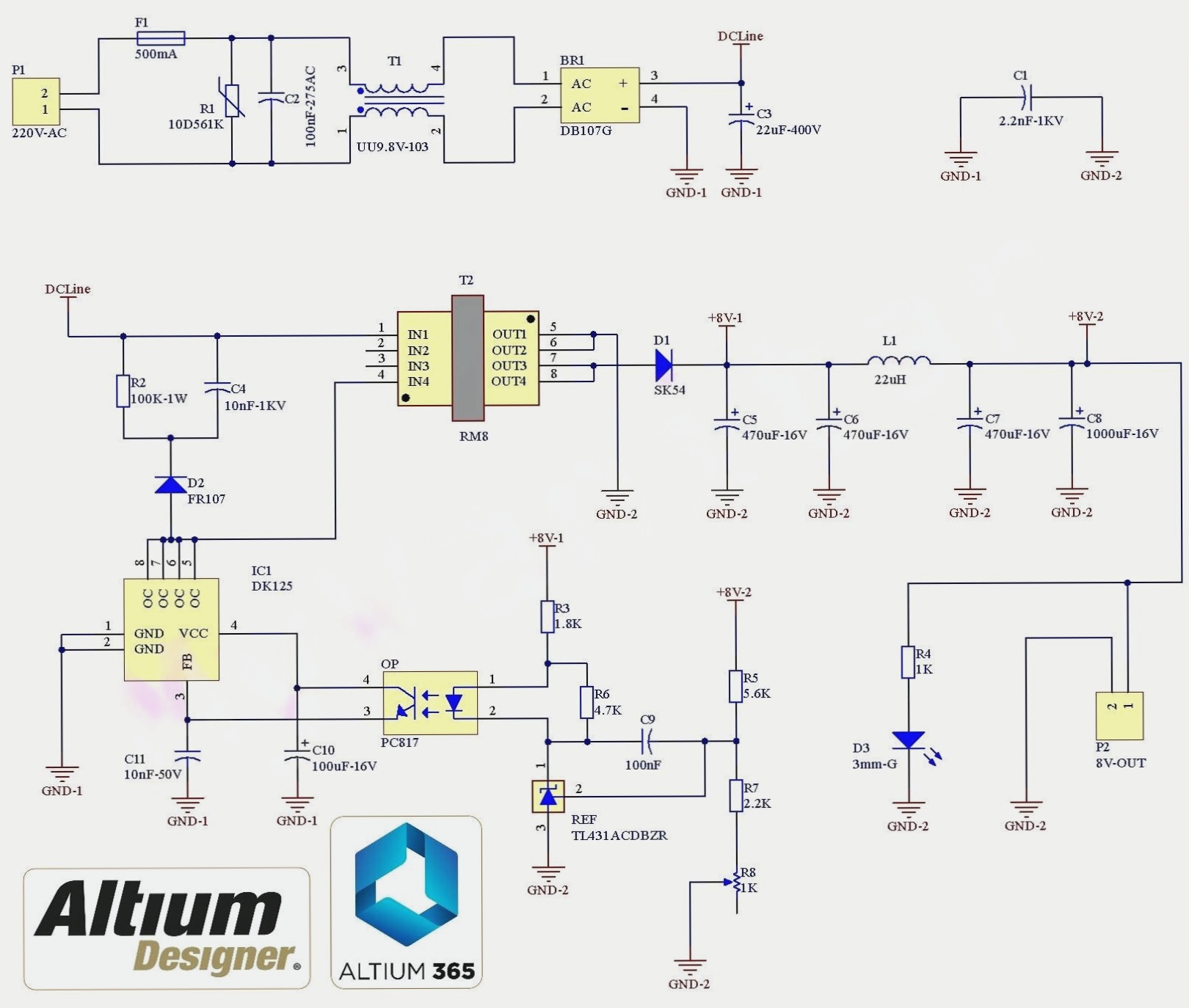
The Importance of Copper Coating in PCB Design
Copper coating plays a vital role in PCB design, whether using local software or international tools like Protel or PowerPCB. The intelligent application of copper coating is essential for reducing ground impedance, enhancing circuit interference resistance, improving power supply efficiency, and minimizing voltage drop. Proper copper coating also helps connect to the ground wire, reducing loop areas and ensuring minimal distortion during soldering.
Copper Pouring and Its Benefits
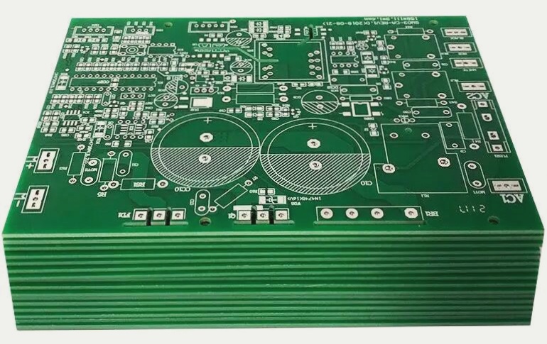
Copper pouring involves filling unused areas of the PCB with solid copper, known as copper filling. This process helps in reducing ground impedance, enhancing current capacity, and providing effective shielding against interference. Improper handling of copper can have detrimental effects, making it crucial to understand the advantages and disadvantages of copper coating.
Effects of Copper Coating at High Frequencies
At high frequencies, the distributed capacitance of traces on a PCB can significantly impact performance. Improper grounding of copper coating can lead to noise emission through traces, affecting circuit operation. Proper management of copper coating is essential in high-frequency circuits to ensure strong connections and effective shielding against interference.
Comparison of Copper Coating Methods
There are two primary methods of copper coating: large-area copper coating and grid copper. Each method serves different purposes, with large-area coating enhancing current capacity and providing shielding, while grid copper is primarily used for shielding and heat dissipation. The choice between the two methods depends on the operational conditions of the circuit board, with considerations for current capacity, shielding, and interference reduction.
Considerations for Effective Copper Plating
- Use the main “ground” as a reference for independent copper pouring when PCB features multiple grounds.
- Consider using 0-ohm resistors, magnetic beads, or inductors for single-point connections between different grounds.
- Apply copper coating near the crystal oscillator to reduce high-frequency emissions, grounding its shell separately for optimal performance.
By understanding the importance of copper coating and implementing the right methods, PCB designers can enhance circuit performance, reduce interference, and improve overall efficiency.
Important Tips for Effective PCB Grounding
- Address the island (dead zone) issue by adding a ground via for a cost-effective solution.
- Treat the ground wire equally at the beginning of routing and ensure proper routing instead of just covering after copper application.
- Avoid sharp corners on the board as they can act as transmitting antennas; opt for rounded edges.
- Avoid applying copper in open areas of the middle layer in multilayer boards for better grounding.
- Ensure solid grounding for metal components like radiators and reinforcement strips within devices.
- Properly ground the heat-dissipating metal block of the three-terminal regulator and the ground isolation strip near the crystal oscillator.
Effectively addressing grounding issues related to copper on the PCB can reduce signal line return area and minimize electromagnetic interference. For any PCB manufacturing needs, feel free to contact us.