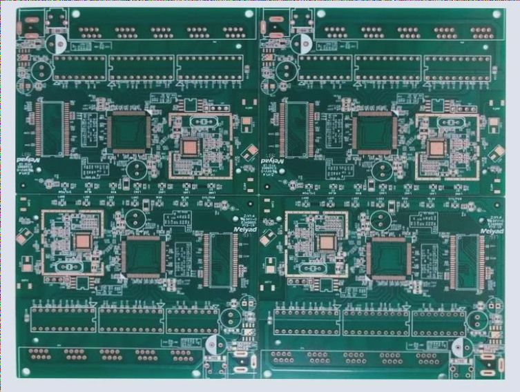
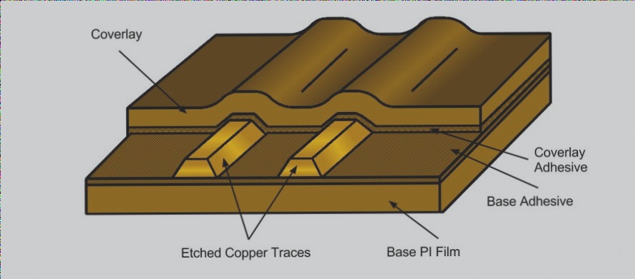
The PCB production process is as follows:
Cutting ->Dry film and roll film ->Exposure ->Development ->Etching ->Film removal ->Drilling ->Copper plating ->Light shielding layer ->Screen printing ->Surface treatment ->Forming ->Electrical measurement, etc. These steps
You may not be familiar with these terms yet, so let’s explain the production process of double-sided panels.
1、 Cutting materials
Cutting is the process of cutting copper-clad laminates into sizes suitable for production line processing. This step is not to cut it into small pieces on the PCB drawing you designed, but to arrange multiple boards according to the PCB drawing and then cut them. After the PCB is completed, proceed with cutting the small pieces.

1. **Dry Film and Film**
A layer of dry film is applied to the copper-clad board. When irradiated with ultraviolet rays, the film cures to form a protective layer on the board. This helps in subsequent exposure and etching away unnecessary copper. Next, the film diagram of our PCB layout is pasted. The film diagram resembles a black-and-white negative of a photo, matching the circuit diagram on the PCB. The film negative’s role is to block ultraviolet light from reaching areas where copper needs to remain. As shown in the image above, the white areas are opaque, while the black areas are transparent and allow light to pass through.
2. **Exposure**
Exposure involves irradiating ultraviolet rays onto the copper-clad laminate with the attached film and dry film. Light passes through the black and transparent parts of the film and impacts the dry film. The dry film cures where light hits, while the areas not exposed remain unchanged.
3. **Development**
Development uses sodium carbonate (the developer, which is weakly alkaline) to dissolve and wash off the unexposed dry film. The exposed dry film remains intact because it has been cured and will not dissolve.
4. **Etching**
In this step, unnecessary copper is etched away using acid copper chloride. Copper covered by the cured dry film remains intact, while uncovered copper is removed, leaving the required circuit lines.
5. **Film Removal**
Film removal involves washing off the cured dry film with sodium hydroxide solution. The uncured dry film was already washed away during development, and different solutions are used to remove the two forms of dry film. At this stage, the circuits reflecting the board’s electrical performance are completed.
6. **Drilling**
Drilling involves creating holes for pads and through holes.
7. **Immersion Copper, Electroplating**
This step plates the walls of pad holes and via holes with a layer of copper, enabling connections through the vias.
8. **Solder Mask**
The solder mask applies a layer of green oil to areas not intended for soldering, preventing external conductivity. This is done through screen printing, followed by light exposure, development, and solder mask application, leaving the pads exposed.
9. **Silk Screen**
Silk-screen printing is used to add component labels, logos, and descriptive text onto the PCB.
10. **Surface Treatment**
Surface treatment prevents copper from oxidizing in the air and includes processes such as hot air leveling (tin spraying), OSP, gold immersion, gold plating, and gold fingers.
11. **Electrical Testing, Sampling, Packaging**
After production, the PCB board undergoes electrical testing to check for open or short circuits. Once testing is complete, the board is ready for packaging and shipping.
The above outlines the PCB production process. For multi-layer boards, a lamination process is also required, which is not detailed here. This overview provides a general understanding of the PCB manufacturing process and its impact on factory production.


