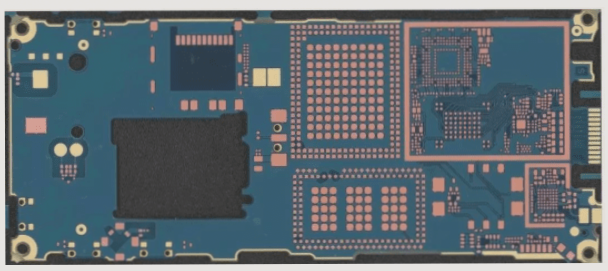
PCB design continues to face challenges as electronic products demand ever more efficient layouts. Engineers must place components strategically to not only meet functional requirements but also adhere to product specifications, including those of the circuit board itself. One of the key challenges is fitting smaller components together while avoiding potential issues during the manufacturing process.
Preparation plays a critical role in achieving successful PCB layout and design outcomes. By identifying design constraints early, engineers can simplify the design process. Key requirements such as component size and placement, as well as tolerances, power, and impedance considerations, can be consolidated into a set of initial design constraints. Establishing these constraints at the outset helps guide the design and minimizes errors, ultimately saving both time and money.
It’s also advisable to maintain a collection of pre-defined design templates and constraints from past projects. These templates, refined through experience, can accelerate the design of new boards or upgrades to existing ones. By reusing proven layouts and settings, designers can avoid reinventing the wheel, ensuring faster turnaround and fewer mistakes.
Once the constraints are established and understood, the layout process becomes less error-prone, leading to more reliable and cost-effective designs. In some cases, advanced layout techniques, such as embedding devices in the inner layers of the PCB, can help reduce board size. However, these strategies should always be evaluated in collaboration with the manufacturer to ensure feasibility and meet all functional requirements.
### 1. Consequences of Poor Planning in PCB Layout
Lack of careful planning or errors in PCB layout specifications can lead to significant issues, both in product quality and functionality. Conflicts between components and circuit paths can result from various factors, such as electromagnetic interference (EMI), inadequate track width, mismatched component sizes, or physical limitations of the board itself. These issues may cause the manufactured product to fail to meet regulatory standards or functional specifications.
Furthermore, when a PCB is not manufacturable according to the original design, back-and-forth revisions between the designer and manufacturer are often required. This not only delays project timelines but also drives up costs. In the worst-case scenario, the engineer may need to completely redesign the PCB, starting from scratch, which can be time-consuming and expensive.
In conclusion, proper planning and early identification of design constraints are essential for creating manufacturable, high-quality PCBs. By incorporating lessons from past designs and working closely with manufacturers, engineers can avoid costly mistakes and ensure that their circuit boards meet both functional and regulatory requirements.

### 1. Overview of PCB Design and Manufacturing Process
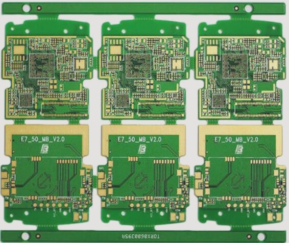
In modern PCB (Printed Circuit Board) production, most designs are created using CAD (Computer-Aided Design) software or specialized PCB design tools. These tools are widely used by technicians and engineers due to their ease of use and familiarity. Once the design is completed, the manufacturer uses automated systems and advanced Computer-Aided Manufacturing (CAM) technology to translate the design files into an actual PCB. However, the design and manufacturing processes may not always be perfectly aligned, which can lead to discrepancies between the intended design and the final product. This misalignment can result in circuit boards that do not perform as expected or are difficult to manufacture, ultimately causing delays and increased production costs.
### 2. Meeting the Needs of Effective PCB Layout
PCB designers face the challenge of not only ensuring that the board performs the required functions but also creating layouts that are optimized for efficient manufacturing. To achieve this, it’s crucial for designers to understand the manufacturing process. By understanding how the production methods interact with their design, engineers can anticipate potential issues and optimize the layout for manufacturability and cost-effectiveness. This is especially important when working with multilayer boards or designs that require complex component placements, such as double-sided laminates. These designs place additional emphasis on Design for Manufacturability (DFM) principles, which are critical for ensuring the final product meets both functional and manufacturing requirements.
### 3. Design for Manufacturability (DFM) in PCB Layout
The placement of components is a key factor in determining whether the final PCB will match the designer’s expectations. In automated manufacturing, the placement of components may differ from the designer’s original intentions, which can affect the overall functionality and assembly process. While the final product may still be functional, there is a risk that it could be more difficult to assemble or repair due to suboptimal component placement. Moreover, the routing of circuit paths can also be altered during manufacturing. While these changes might not render the PCB unusable, they could make it more challenging to install or service compared to the initial design.
### 4. Leveraging DFM Tools for Better Designs
Before creating prototypes, PCB designers can leverage DFM (Design for Manufacturability) software to ensure the design is optimized for production. DFM tools analyze the design files and identify potential manufacturing issues, such as component placement conflicts, trace width violations, or other manufacturability concerns. By using both traditional PCB design software and DFM applications in tandem, designers can ensure that their boards are not only functional but also cost-effective and easy to manufacture. This integrated approach helps reduce the risk of delays, production errors, and costly design modifications.
### Conclusion
In conclusion, the process of PCB design and manufacturing requires close attention to both functional and manufacturability aspects. Designers must not only focus on creating a circuit board that performs well but also consider the complexities of the manufacturing process. By incorporating DFM principles and using appropriate design and analysis tools, designers can significantly enhance the quality, efficiency, and cost-effectiveness of their PCB designs, leading to better products and smoother production workflows.
Preparation plays a critical role in achieving successful PCB layout and design outcomes. By identifying design constraints early, engineers can simplify the design process. Key requirements such as component size and placement, as well as tolerances, power, and impedance considerations, can be consolidated into a set of initial design constraints. Establishing these constraints at the outset helps guide the design and minimizes errors, ultimately saving both time and money.
It’s also advisable to maintain a collection of pre-defined design templates and constraints from past projects. These templates, refined through experience, can accelerate the design of new boards or upgrades to existing ones. By reusing proven layouts and settings, designers can avoid reinventing the wheel, ensuring faster turnaround and fewer mistakes.
Once the constraints are established and understood, the layout process becomes less error-prone, leading to more reliable and cost-effective designs. In some cases, advanced layout techniques, such as embedding devices in the inner layers of the PCB, can help reduce board size. However, these strategies should always be evaluated in collaboration with the manufacturer to ensure feasibility and meet all functional requirements.
### 1. Consequences of Poor Planning in PCB Layout
Lack of careful planning or errors in PCB layout specifications can lead to significant issues, both in product quality and functionality. Conflicts between components and circuit paths can result from various factors, such as electromagnetic interference (EMI), inadequate track width, mismatched component sizes, or physical limitations of the board itself. These issues may cause the manufactured product to fail to meet regulatory standards or functional specifications.
Furthermore, when a PCB is not manufacturable according to the original design, back-and-forth revisions between the designer and manufacturer are often required. This not only delays project timelines but also drives up costs. In the worst-case scenario, the engineer may need to completely redesign the PCB, starting from scratch, which can be time-consuming and expensive.
In conclusion, proper planning and early identification of design constraints are essential for creating manufacturable, high-quality PCBs. By incorporating lessons from past designs and working closely with manufacturers, engineers can avoid costly mistakes and ensure that their circuit boards meet both functional and regulatory requirements.
### 1. Overview of PCB Design and Manufacturing Process
In modern PCB (Printed Circuit Board) production, most designs are created using CAD (Computer-Aided Design) software or specialized PCB design tools. These tools are widely used by technicians and engineers due to their ease of use and familiarity. Once the design is completed, the manufacturer uses automated systems and advanced Computer-Aided Manufacturing (CAM) technology to translate the design files into an actual PCB. However, the design and manufacturing processes may not always be perfectly aligned, which can lead to discrepancies between the intended design and the final product. This misalignment can result in circuit boards that do not perform as expected or are difficult to manufacture, ultimately causing delays and increased production costs.
### 2. Meeting the Needs of Effective PCB Layout
PCB designers face the challenge of not only ensuring that the board performs the required functions but also creating layouts that are optimized for efficient manufacturing. To achieve this, it’s crucial for designers to understand the manufacturing process. By understanding how the production methods interact with their design, engineers can anticipate potential issues and optimize the layout for manufacturability and cost-effectiveness. This is especially important when working with multilayer boards or designs that require complex component placements, such as double-sided laminates. These designs place additional emphasis on Design for Manufacturability (DFM) principles, which are critical for ensuring the final product meets both functional and manufacturing requirements.
### 3. Design for Manufacturability (DFM) in PCB Layout
The placement of components is a key factor in determining whether the final PCB will match the designer’s expectations. In automated manufacturing, the placement of components may differ from the designer’s original intentions, which can affect the overall functionality and assembly process. While the final product may still be functional, there is a risk that it could be more difficult to assemble or repair due to suboptimal component placement. Moreover, the routing of circuit paths can also be altered during manufacturing. While these changes might not render the PCB unusable, they could make it more challenging to install or service compared to the initial design.
### 4. Leveraging DFM Tools for Better Designs
Before creating prototypes, PCB designers can leverage DFM (Design for Manufacturability) software to ensure the design is optimized for production. DFM tools analyze the design files and identify potential manufacturing issues, such as component placement conflicts, trace width violations, or other manufacturability concerns. By using both traditional PCB design software and DFM applications in tandem, designers can ensure that their boards are not only functional but also cost-effective and easy to manufacture. This integrated approach helps reduce the risk of delays, production errors, and costly design modifications.
### Conclusion
In conclusion, the process of PCB design and manufacturing requires close attention to both functional and manufacturability aspects. Designers must not only focus on creating a circuit board that performs well but also consider the complexities of the manufacturing process. By incorporating DFM principles and using appropriate design and analysis tools, designers can significantly enhance the quality, efficiency, and cost-effectiveness of their PCB designs, leading to better products and smoother production workflows.
If you have any questions about PCB or PCBA, feel free to reach out to me at info@wellcircuits.com.