Understanding PCB Assembly Processes
Curious about PCB assembly processes and how they benefit PCB assembly services? Let’s delve into the world of PCB assembly to gain a better understanding of how it all works.
A PCB assembly process marks the final stage of PCB design before a product is ready for shipment. This crucial step solidifies the product design, making it essential to choose a board assembly company that offers top-notch services.
The PCB assembly service involves soldering or assembling electronic components onto a PCB (printed circuit board). This intricate process can be carried out manually, by machines, or through reflow ovens.
Before diving into the assembly process, meticulous attention to detail is required to ensure the quality and functionality of the final product, especially for PCBs with numerous components.
Preparation Before Assembly
Prior to commencing the assembly process, engineers scrutinize the design to fabricate it effectively, utilizing specialized software to create a blueprint. Prototypes are then developed for testing before mass production, saving time, money, and effort in the long run.
Ordering necessary parts in advance is crucial to streamline the manufacturing process, given the variety of components used on a single circuit board.
Once the PCB design is finalized, it is sent to a manufacturer who fabricates the bare PCB using copper foil, fiberglass, and epoxy resin layers. The PCB manufacturing process typically involves two main stages:
- PCB Fabrication Process: Creating copper foil patterns on an epoxy board based on the design’s Gerber files.
- PCB Assembly Process: Attaching components like integrated circuits, switches, and connectors to the fabricated panel.
Upon completing both processes, a fully functional printed circuit board assembly is achieved!
Overview of PCB Assembly Process
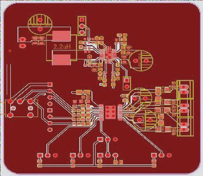
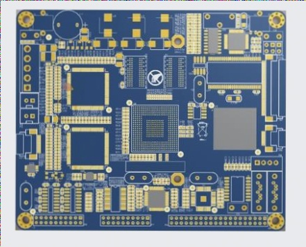
PCB assembly, also known as PCBA, entails soldering electronic components onto a PCB to form a functional printed circuit assembly (PCA). A PCB is a thin board made of fiberglass, composite epoxy, or laminate materials with copper tracks connecting various components.
Electronic parts are mounted on the PCB’s surface, with some specialized boards featuring internal layers. The assembly process involves mounting passive (resistors, capacitors) and active (transistors, microchips) components, which can be surface mounted or through-hole mounted based on their size and functionality.
Visualizing the PCB assembly process can be complex for newcomers to electronics manufacturing. Here’s a simplified overview of the key steps involved:
- Component Preparation: Preparing components by forming leads for insertion into plated through holes (PTH) on the board.
- Board Handling: Inspecting and cleaning the bare board to eliminate contaminants before the surface mounting technology (SMT) phase begins.
PCB Assembly Process Overview
- Surface Mounting Technology (SMT):
- Automated Optical Inspection (AOI):
Components are placed on the surface of the bare board using a pick and place machine. Solder paste is applied to each component pad before placement. The boards then enter a reflow oven where the solder paste melts, joining components to the board.
After reflow soldering is complete, the boards are inspected using an AOI machine that takes photographs of each side of every board and compares them to specifications for missing or incorrectly placed components. Any panels with incorrect placements or missing parts are flagged for repair/re-work.
Key Steps in PCBA Process
- Solder Paste:
- Pick and Place:
- Soldering:
- Reflow Oven:
- Wave Soldering:
- Cleaning:
- Inspection:
- Manual Checks:
The bare etched PCB is first placed on a “sticky” jig with adhesive to hold it in place. A solder paste stencil is used to apply solder paste to the pads, essential for joining SMT components to the board.
SMD components are picked up and placed precisely on the pads using a pick and place machine with high accuracy. The CNC system controls the exact location of each component based on CAD data.
Components are soldered onto the PCB using a soldering iron, ensuring a secure connection. Solder joints are melted in a reflow oven to form strong bonds.
Reflow soldering is achieved by heating the board in an oven to melt the solder paste. The temperature profile is crucial for proper flow and connection of components.
Double-sided PCBs are assembled using wave soldering, where the board passes over a wave of molten solder to adhere components to both sides.
Excess solder paste is removed from the PCB through a cleaning process to prevent short circuits and ensure reliability of the board.
The quality of solder paste printing, component placement, and soldering is inspected to ensure high-quality PCB assembly and improve board reliability.
PCB Assembly Inspection Methods
- Manual Inspection:
Manual inspection involves time-consuming checks during various stages of PCB assembly, including array testing, component placement, soldering, cleaning, conformal coating, and final inspection.
Automatic Optical Inspection (AOI)
Automated optical inspection systems utilize cameras to visually inspect PCBs before and after component placement. These systems detect faults like solder bridges, missing components, incorrect component positions, and broken traces on the PCB substrate.
X-ray Inspection
X-ray inspection is crucial for detecting defects in BGA packages that are not visible through optical inspection methods. Common issues identified include tombstoning, lifted pads, solder joint cracks, and voids in solder balls.
PCB Assembly Testing and Feedback
- Test:
Testing is essential for complex PCB assembly jobs and involves using devices like Flying probe, bed-of-nails, and fixtureless test (In-circuit testing) to ensure functionality.
- Feedback:
Feedback plays a vital role in enhancing future PCB assembly quality by pinpointing factors leading to defects, such as design, manufacturing, and material issues.

After PCB Assembly Process
The post-PCBA process is the final step in PCB assembly, involving tests like In-circuit testing and Functional Testing to ensure proper functionality.
In-Circuit Test
This initial test checks every component on the board using a tester machine, allowing for replacement of faulty pieces before further testing.
1. With Flying Probe:
A flying probe tester scans the entire PCB for short circuits, open circuits, incorrect component placement, and polarity, making it suitable for low-volume production runs and prototypes.
2. With Fixtured Test:
A fixture bed tailored to the PCB allows for accurate testing using a tester machine and component mounting.
3. Functional Test
This test ensures all components work together correctly to achieve the desired function, such as powering on or data transfer.
Key Takeaway
PCB assembly is intricate and demands meticulous attention to detail to avoid costly mistakes. Establishing a streamlined assembly process tailored to your company can help prevent errors and enhance efficiency. Whether considering outsourcing or in-house assembly, understanding the PCB assembly process is crucial for making informed decisions.