The Importance of PCB Component Layout in SMT Production
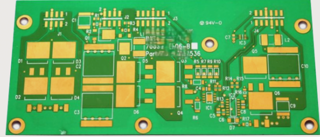
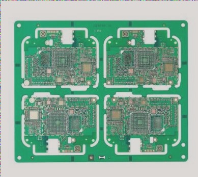
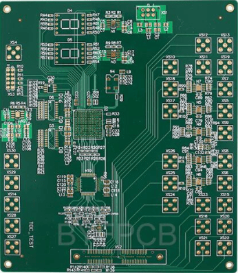
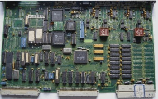
Proper arrangement of components on a PCB is crucial for meeting electrical performance, mechanical structure requirements, and aligning with SMT production standards. Design-related quality issues can be challenging to rectify during production, emphasizing the need for PCB design engineers to understand SMT process characteristics.
Circuit Design Requirements for Component Layout
Component layout significantly impacts PCB performance. Large circuits should be segmented into unit circuits, with each unit’s position organized based on signal flow direction. It’s essential to avoid signal overlap and maintain a consistent signal flow direction to facilitate fault detection.

SMT Process Requirements for Component Layout Design
Components must be arranged according to SMT production equipment and processes. Layout requirements vary based on the soldering method used, such as reflow or wave soldering. Different layout requirements exist for double-sided reflow soldering on primary and secondary surfaces.
Key Requirements for a Reasonable PCB Layout Design:
- The distribution of components should be uniform.
- Similar components should be oriented in the same direction for ease of mounting, soldering, and testing.
- Maintain adequate space around larger components for effective operation of SMD rework equipment.
- Position heating elements away from other components, preferably in corners and well-ventilated areas.
- Keep temperature-sensitive components away from heating elements.
- Place components requiring frequent adjustment in easily accessible positions.
- Locate fixing holes near stress-prone areas and provide adequate space around them.
- Add additional clearance for components requiring secondary processing due to tolerances.
- Avoid placing valuable components in high-stress areas prone to cracks.
The reasonableness of the layout directly impacts wiring effectiveness, making a well-considered PCB layout essential for successful design. For any PCB manufacturing needs, feel free to contact us.


