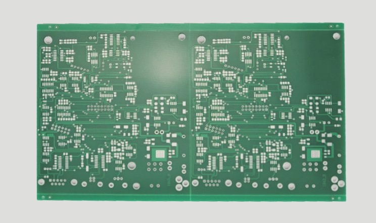
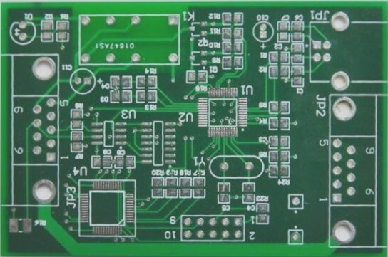
PCB Proofing Process Overview
PCB proofing, also known as PCB prototype production, is a crucial step in the manufacturing of printed circuit boards. It involves testing the design and functionality of the PCB before mass production. The process typically includes the following steps:
1. Contacting the Manufacturer
- Provide necessary documents, process requirements, and quantities to the manufacturer.
- Receive a quote, place orders, and track production progress.
2. Cutting
- Objective: Cut large sheets into smaller pieces to meet engineering data and customer specifications.
- Process: Cut board according to requirements, grind, and finish.
3. Drilling
- Objective: Drill apertures at specified positions based on engineering data.
- Process: Stack boards, drill, inspect, and repair if needed.
4. Sink Copper
- Objective: Deposit a thin layer of copper on insulating hole walls.
- Process: Rough grinding, copper sinking, chemical treatment.
5. Graphics Transfer
Transfer images from production film to the board.

- Process: Printing, drying, developing, and inspecting.
6. Graphic Plating
- Objective: Deposit required copper and gold-nickel/tin layers.
- Process: Degreasing, etching, plating, and washing.
7. Film Removal
- Objective: Remove anti-plating coating film to expose copper layers.
- Process: Soaking, rinsing, and scrubbing.
8. Etching
Use chemical reaction to corrode non-circuit copper areas.
9. Green Oil Application
- Objective: Transfer green oil film to protect the circuit during soldering.
- Process: Printing, curing, and exposing.
10. Character Printing
- Objective: Provide identification marks.
- Process: Printing characters for easy identification.
11. Gold-Plated Fingers
- Objective: Plate nickel/gold for hardness and wear resistance.
- Process: Degreasing, plating, and washing.
12. Tin Plating
- Objective: Coat exposed copper surfaces for corrosion protection.
- Process: Coating, leveling, and drying.