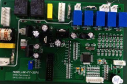
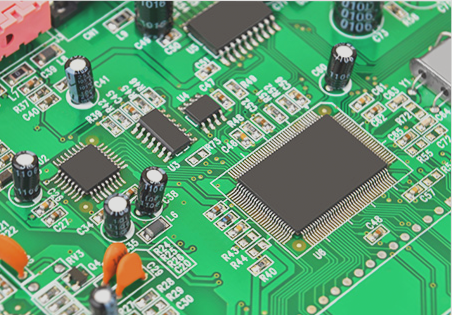
The LVDS signal is not only a differential signal but also a high-speed digital signal. Therefore, whether the LVDS transmission medium employs a PCB trace or a cable, it is essential to implement measures that prevent signal reflection at the media terminal while minimizing electromagnetic interference to maintain signal integrity. By considering these factors in PCB layout design, creating high-speed differential circuit boards becomes manageable.
The following briefly outlines the key design considerations for PCB design related to LVDS signals:
1. Utilize a multi-layer board. Circuit boards for LVDS signals are typically designed as multi-layer boards. Given that LVDS signals are high-speed, an adjacent ground layer should be included to shield the LVDS signal and reduce interference. For lower-density boards, it is advisable to place LVDS signals on separate layers from other signals whenever possible. For instance, in a four-layer board, the arrangement can typically be: LVDS signal layer, ground layer, power layer, and other signal layers.
2. Calculate and control LVDS signal impedance. The voltage swing of the LVDS signal is only 350mV, making it suitable for current-driven differential signal operation. To ensure that the signal remains unaffected by reflections during propagation in the transmission line, it is crucial to control the transmission line impedance, with differential impedance typically set at 100 ± 10Ω. The effectiveness of impedance control significantly impacts signal integrity and delay.

**Simulation Analysis of Serial LVDS Signal**
This analysis highlights key considerations when designing LVDS signals. While adhering to general rules in PCB design, achieving correctness and accuracy requires comprehensive signal simulation. Through simulation, crosstalk, delay, reflection, and eye pattern waveforms can be evaluated to ensure design integrity. The simulation process for signal integrity begins by establishing a model for the components, followed by pre-simulation to ascertain wiring parameters and constraints. Design adjustments are made during the physical realization stage, culminating in post-simulation to confirm compliance with design requirements. The model’s accuracy throughout this process significantly impacts simulation outcomes, and the methods employed in both pre- and post-simulation stages are crucial. This design utilizes a highly accurate SPICE model. The following outlines the implementation process of simulation in this project.
1. **PCB Stack Setup**
Based on the above analysis, the stacking configuration of the PCB is critical for signal coupling and impedance calculations. Thus, stacking design must precede PCB design, followed by impedance calculations for the signals. The laminated design for this project is illustrated below:
Due to high PCB density, this design employs a 10-layer laminate structure. After strategically arranging laminate thickness, Allegro calculations indicate that the differential line width for surface microstrip and inner strip line is 6 mils with a spacing of 6 mils, yielding theoretical impedance values of 100.1Ω and 98.8Ω, respectively.
2. **Setting the DC Voltage Value**
This step involves specifying the DC voltage for certain networks (typically power ground) to determine the voltage to be applied and to facilitate EMI simulation. Identifying one or more voltage source pins is essential, with voltage values including reference information utilized by the model during simulation.
3. **Device Settings**
During Allegro simulation, devices are categorized into three types: ICs, connectors, and discrete components (resistors, capacitors, etc.). Allegro assigns simulation attributes to device pins based on type; for discrete devices and connector pins, the attribute is UPSPEC, while IC pins can be classified as IN, OUT, or BI.
4. **Model Allocation**
The primary models used in high-speed PCB simulation are device models and transmission line models. Device models are typically provided by manufacturers. For high-speed serial signals, a higher-precision SPICE model is used for analysis. Transmission line models are developed via simulation software. The transmission line’s impact on signal integrity is pronounced, so the simulation software’s accuracy in modeling these lines is crucial. Differential pair line models include stripline and microstrip configurations, where both signal and return paths exhibit finite resistance, influenced by the length and cross-sectional area of the transmission line.
5. **SI Inspection**
The SI Audit function checks whether a specific network or group of networks can be analyzed. This typically involves identifying high-speed networks of interest, with a primary focus on LVDS serial signals.
6. **Extracting Network Topology**
Extract the topological structure of the relevant signal from the PCB, which encompasses the driving and receiving ends, transmission lines, and associated matching resistors and capacitors. The topology reveals the signal’s pathways, impacting transmission quality.
7. **Viewing the Waveform**
After completing the aforementioned steps, simulations can commence. Allegro supports signal reflection and crosstalk simulations, with eye diagram analysis required for differential lines. Simulations are categorized into pre- and post-simulation phases. When using Allegro for PCB design, it is essential to adjust the design in real-time based on simulation results to meet specifications.
In wiring differential pairs, two key considerations must be noted. Firstly, the lengths of both lines should be equal to ensure the differential signals maintain opposite polarities consistently, minimizing common mode components. Secondly, the distance between the two lines (determined by differential impedance) must remain constant, meaning they should be kept parallel. This parallelism can be achieved either side-by-side on the same layer or on adjacent layers (over-under), with side-by-side implementations being more common. Maintaining equidistance is crucial for achieving uniform differential impedance and reducing reflections.
From this analysis, it’s evident that high-speed serial signal design requires careful consideration not only of circuit design but also of PCB layout and simulation analysis. As signal frequencies increase, the complexities related to delay, crosstalk, and signal integrity multiply, making management of these factors increasingly challenging. Engineers must thoroughly analyze wiring designs, rely on accurate models, effective simulations, and scientific methods to provide sound guidance for complex high-speed designs, reduce correction cycles, and ensure successful PCB design.
The following briefly outlines the key design considerations for PCB design related to LVDS signals:
1. Utilize a multi-layer board. Circuit boards for LVDS signals are typically designed as multi-layer boards. Given that LVDS signals are high-speed, an adjacent ground layer should be included to shield the LVDS signal and reduce interference. For lower-density boards, it is advisable to place LVDS signals on separate layers from other signals whenever possible. For instance, in a four-layer board, the arrangement can typically be: LVDS signal layer, ground layer, power layer, and other signal layers.
2. Calculate and control LVDS signal impedance. The voltage swing of the LVDS signal is only 350mV, making it suitable for current-driven differential signal operation. To ensure that the signal remains unaffected by reflections during propagation in the transmission line, it is crucial to control the transmission line impedance, with differential impedance typically set at 100 ± 10Ω. The effectiveness of impedance control significantly impacts signal integrity and delay.

**Simulation Analysis of Serial LVDS Signal**
This analysis highlights key considerations when designing LVDS signals. While adhering to general rules in PCB design, achieving correctness and accuracy requires comprehensive signal simulation. Through simulation, crosstalk, delay, reflection, and eye pattern waveforms can be evaluated to ensure design integrity. The simulation process for signal integrity begins by establishing a model for the components, followed by pre-simulation to ascertain wiring parameters and constraints. Design adjustments are made during the physical realization stage, culminating in post-simulation to confirm compliance with design requirements. The model’s accuracy throughout this process significantly impacts simulation outcomes, and the methods employed in both pre- and post-simulation stages are crucial. This design utilizes a highly accurate SPICE model. The following outlines the implementation process of simulation in this project.
1. **PCB Stack Setup**
Based on the above analysis, the stacking configuration of the PCB is critical for signal coupling and impedance calculations. Thus, stacking design must precede PCB design, followed by impedance calculations for the signals. The laminated design for this project is illustrated below:
Due to high PCB density, this design employs a 10-layer laminate structure. After strategically arranging laminate thickness, Allegro calculations indicate that the differential line width for surface microstrip and inner strip line is 6 mils with a spacing of 6 mils, yielding theoretical impedance values of 100.1Ω and 98.8Ω, respectively.
2. **Setting the DC Voltage Value**
This step involves specifying the DC voltage for certain networks (typically power ground) to determine the voltage to be applied and to facilitate EMI simulation. Identifying one or more voltage source pins is essential, with voltage values including reference information utilized by the model during simulation.
3. **Device Settings**
During Allegro simulation, devices are categorized into three types: ICs, connectors, and discrete components (resistors, capacitors, etc.). Allegro assigns simulation attributes to device pins based on type; for discrete devices and connector pins, the attribute is UPSPEC, while IC pins can be classified as IN, OUT, or BI.
4. **Model Allocation**
The primary models used in high-speed PCB simulation are device models and transmission line models. Device models are typically provided by manufacturers. For high-speed serial signals, a higher-precision SPICE model is used for analysis. Transmission line models are developed via simulation software. The transmission line’s impact on signal integrity is pronounced, so the simulation software’s accuracy in modeling these lines is crucial. Differential pair line models include stripline and microstrip configurations, where both signal and return paths exhibit finite resistance, influenced by the length and cross-sectional area of the transmission line.
5. **SI Inspection**
The SI Audit function checks whether a specific network or group of networks can be analyzed. This typically involves identifying high-speed networks of interest, with a primary focus on LVDS serial signals.
6. **Extracting Network Topology**
Extract the topological structure of the relevant signal from the PCB, which encompasses the driving and receiving ends, transmission lines, and associated matching resistors and capacitors. The topology reveals the signal’s pathways, impacting transmission quality.
7. **Viewing the Waveform**
After completing the aforementioned steps, simulations can commence. Allegro supports signal reflection and crosstalk simulations, with eye diagram analysis required for differential lines. Simulations are categorized into pre- and post-simulation phases. When using Allegro for PCB design, it is essential to adjust the design in real-time based on simulation results to meet specifications.
In wiring differential pairs, two key considerations must be noted. Firstly, the lengths of both lines should be equal to ensure the differential signals maintain opposite polarities consistently, minimizing common mode components. Secondly, the distance between the two lines (determined by differential impedance) must remain constant, meaning they should be kept parallel. This parallelism can be achieved either side-by-side on the same layer or on adjacent layers (over-under), with side-by-side implementations being more common. Maintaining equidistance is crucial for achieving uniform differential impedance and reducing reflections.
From this analysis, it’s evident that high-speed serial signal design requires careful consideration not only of circuit design but also of PCB layout and simulation analysis. As signal frequencies increase, the complexities related to delay, crosstalk, and signal integrity multiply, making management of these factors increasingly challenging. Engineers must thoroughly analyze wiring designs, rely on accurate models, effective simulations, and scientific methods to provide sound guidance for complex high-speed designs, reduce correction cycles, and ensure successful PCB design.


