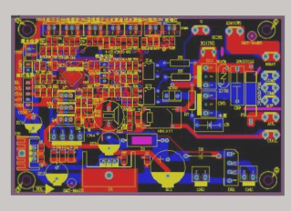
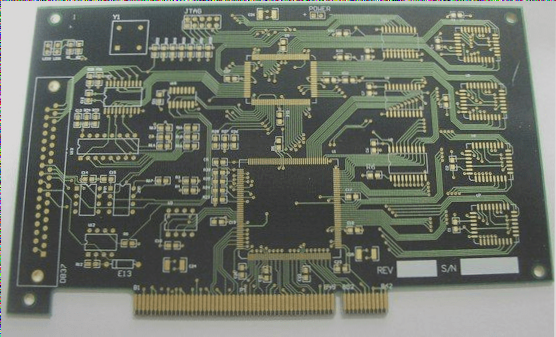
Positioning Holes in PCB Manufacturing and Assembly
In PCB design and assembly processes, it is crucial to include two to three positioning holes at the corners for proper alignment.
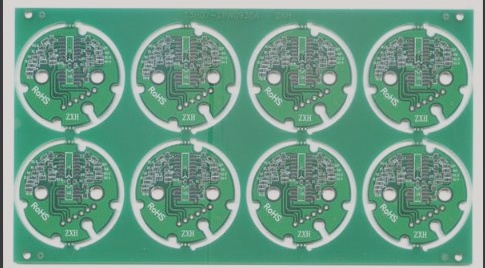
Effective Use of PCB Splicing for Enhanced Production Efficiency
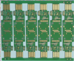
When dealing with small or irregularly shaped PCBs, splicing multiple smaller boards together can create a larger, more manageable PCB. This method improves processing efficiency and is commonly used in the industry.
- Joining smaller PCBs to create larger panels falls within the ideal processing range, making them suitable for automated assembly.
- Yin-Yang splicing, a technique involving SMDs on both sides, reduces costs and improves PCB programming efficiency.
- Various methods like V-slots and round holes can be used to connect sub-boards, enhancing the splicing process.
- Stencil mesh patterns can also be utilized for cost-effective splicing, especially for small batch production.
Design Considerations for Testability in SMT
Testability design in SMT focuses on addressing potential testing challenges during product manufacturing, emphasizing process and electrical design aspects.
Process Design Requirements
- Positioning accuracy, substrate size, and probe type influence detection reliability.
- Precise positioning holes with an error tolerance of ±0.05mm are essential for accurate testing.
- Test points should have a minimum diameter of 0.4mm and be placed at least 1.0mm away from components.
- Avoid placing components taller than *mm on the test surface to prevent interference with probe contact.
- Test points must not be covered by solder resist or ink markings to ensure reliable contact.
Best Practices for PCB Test Point Placement
- Route SMC/SMD test points from component surface to soldering side via vias with hole diameters over 1mm for cost-effective online testing.
- Ensure each electrical node has a corresponding test point, with dedicated POWER and GROUND test points near ICs ideally within 2.54mm.
- Increase trace width to 40 mils when placing test points on circuit traces to accommodate probes.
- Evenly distribute test points across PCB to prevent deformation from concentrated probe pressure.
- Include test break points in power supply circuit at various locations for efficient fault detection.
- Use extension wires or via pads for test pads near component leads to avoid the “fault masking effect.”
- Be cautious of probe sway to prevent damage to components during testing.
These guidelines aim to enhance PCB layout manufacturability, improving testing quality and reliability.
If you have any PCB inquiries, feel free to reach out to us at info@wellcircuits.com.