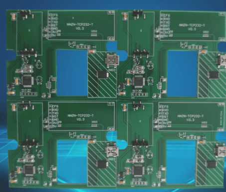
PCB Design Steps Using KiCad
When creating a PCB using KiCad, the process typically involves the following steps:
- Start by designing the schematic in Eeschema.
- Assign footprints to each component on the schematic.
- Utilize Pcbnew to arrange and route the footprints, crafting the actual PCB layout.
Enhancing PCB Design with Additional Pads
While designing a PCB, there are various scenarios where adding extra soldering pads can be beneficial:
- Include pads for test points like oscilloscope or multimeter probes on traces.
- Add extra pads to accommodate different component lead spacings for mounting flexibility.
- Designate areas for a universal grid of pads to aid in future modifications or prototyping.
Streamlining Pad Addition in KiCad
Traditionally, adding pads in Pcbnew involved a cumbersome process of creating corresponding components in Eeschema for each pad. This method becomes impractical for designs requiring numerous pads.
A simpler approach involves using vias that can be converted into pads directly within Pcbnew.
Utilizing Vias for Easy Pad Addition
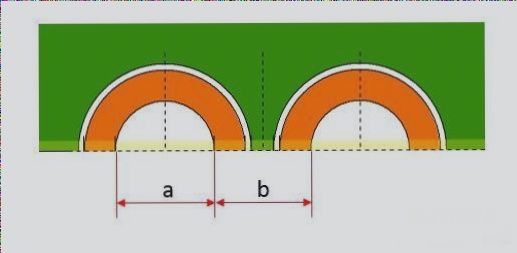
Vias, circular pads with drill holes, can be transformed into solderable pads by exposing copper layers. Here’s how:
After placing vias, create masks in the F.Mask or B.Mask layers to expose copper, turning vias into solderable pads.
By shifting masks, you can control the exposed copper areas on both sides of the PCB.
Benefits of Vias-to-Pads Conversion
Converting vias to pads offers several advantages:
Eliminates the need to add components in Eeschema for pad creation.
Allows flexibility in pad placement anywhere on the PCB in Pcbnew.
The Flexibility and Ease of Using Vias in PCB Design
Vias in PCB design are incredibly versatile. You have the ability to adjust their diameter and drill size, making them suitable for various applications. When utilizing vias as pads, it’s advisable to begin with a larger via and then incorporate the circular mask as previously outlined.
Enhanced Footprint Management
Updating footprints in Pcbnew automatically removes footprints not found in Eeschema. Unlike footprints, vias are not deleted automatically, providing a more consistent design environment.
Efficient Solder Pad Placement
This approach grants you the freedom to place solder pads anywhere on the PCB. For scenarios requiring numerous pads, like a universal grid pattern, you can easily duplicate the via-mask configuration as necessary.
Recommended Method for PCB Design
Overall, this technique is highly recommended due to its user-friendly nature and adaptability in PCB design.
Give It a Try!
We strongly encourage you to experiment with this method. Should you have any inquiries about PCB design or assembly, don’t hesitate to reach out to us at info@wellcircuits.com.