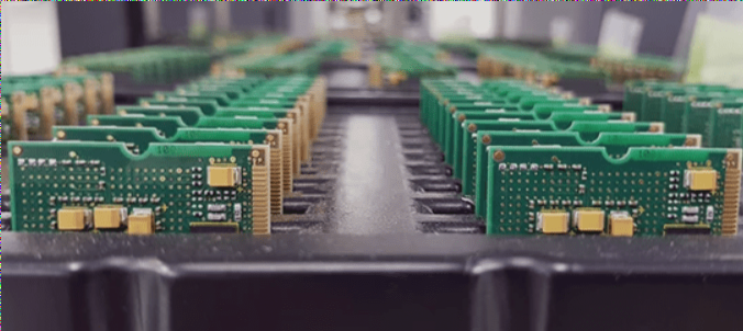
1. For PCB copy boards, even slight carelessness can lead to deformation of the bottom plate.
2. If not addressed, this deformation can negatively impact the quality and performance of the PCB copy board.
3. Directly discarding the deformed board results in additional costs and waste.
4. Here are some methods to correct the deformation of the bottom plate.

1. **Splicing Method**
For graphics with simple lines, large line widths and spacing, and irregular deformations, cut the deformed part of the negative film, resplice the holes according to the hole positions of the drill test board, and then make a copy. This method is suitable for deformed lines, simple graphics, large line widths and spacings, and irregularly deformed graphics. However, it is not suitable for negatives with high wire density and line widths and spacings less than 0.2 mm. When splicing, minimize damage to the wires and avoid affecting the pads. After splicing and copying, carefully check the correctness of the connection relationships. This method works best for films that are not too densely packed and where the deformation of each layer varies. It is particularly effective for correcting solder mask films and power supply layer films in multilayer boards.
2. **Printed Circuit Board Copy Board for Changing Hole Positions**
When using a digital programming instrument, start by comparing the negative film with the drilling test board. Measure and record the length and width of the drilling test board, and then use the digital programming instrument to adjust the hole positions based on the size and deformation. Adjust the drilling test board to align with the deformed negative. The advantage of this method is that it avoids the tedious task of editing negatives and ensures the integrity and quality of the graphics. However, it is less effective for negative films with severe local deformation or uneven deformation. To use this method effectively, you must be proficient in operating the digital programming instrument. After adjusting the hole positions, reset any out-of-tolerance holes to maintain performance. This method is suitable for correcting negative films with dense lines or uniform deformation across each layer.
3. **Pad Overlap Method**
Enlarge the holes on the test board into pads to overlap and deform the circuit piece, ensuring the technical requirements for ring width. After overlapping and copying, the pad will appear elliptical, and there may be halo and deformation effects along the line and disk edge. If the user has very strict requirements for PCB appearance, use this method with caution. It is suitable for films with line widths and spacings greater than 0.30 mm, and where the pattern lines are not too dense.
4. **Photography**
Use a camera to enlarge or reduce the deformed graphics. This method often involves significant film loss and requires multiple adjustments to achieve a satisfactory circuit pattern. Ensure precise focus to avoid line deformation. This method is only suitable for silver salt films and is applicable when re-drilling the test board is inconvenient, provided the deformation ratios in the length and width directions are the same.
5. **Hanging Method**
Due to the physical changes in negative film with environmental temperature and humidity, take it out of the sealed bag before copying and hang it for 4-8 hours in the working environment conditions. This allows the negative film to stabilize before copying, minimizing further deformation. For already deformed film, other measures are necessary. Ensure that the hanging environment’s humidity and temperature match the working conditions, and keep the environment ventilated and dark to prevent contamination. This method is suitable for negative films that have not yet deformed and can also help prevent deformation after copying.
2. If not addressed, this deformation can negatively impact the quality and performance of the PCB copy board.
3. Directly discarding the deformed board results in additional costs and waste.
4. Here are some methods to correct the deformation of the bottom plate.

1. **Splicing Method**
For graphics with simple lines, large line widths and spacing, and irregular deformations, cut the deformed part of the negative film, resplice the holes according to the hole positions of the drill test board, and then make a copy. This method is suitable for deformed lines, simple graphics, large line widths and spacings, and irregularly deformed graphics. However, it is not suitable for negatives with high wire density and line widths and spacings less than 0.2 mm. When splicing, minimize damage to the wires and avoid affecting the pads. After splicing and copying, carefully check the correctness of the connection relationships. This method works best for films that are not too densely packed and where the deformation of each layer varies. It is particularly effective for correcting solder mask films and power supply layer films in multilayer boards.
2. **Printed Circuit Board Copy Board for Changing Hole Positions**
When using a digital programming instrument, start by comparing the negative film with the drilling test board. Measure and record the length and width of the drilling test board, and then use the digital programming instrument to adjust the hole positions based on the size and deformation. Adjust the drilling test board to align with the deformed negative. The advantage of this method is that it avoids the tedious task of editing negatives and ensures the integrity and quality of the graphics. However, it is less effective for negative films with severe local deformation or uneven deformation. To use this method effectively, you must be proficient in operating the digital programming instrument. After adjusting the hole positions, reset any out-of-tolerance holes to maintain performance. This method is suitable for correcting negative films with dense lines or uniform deformation across each layer.
3. **Pad Overlap Method**
Enlarge the holes on the test board into pads to overlap and deform the circuit piece, ensuring the technical requirements for ring width. After overlapping and copying, the pad will appear elliptical, and there may be halo and deformation effects along the line and disk edge. If the user has very strict requirements for PCB appearance, use this method with caution. It is suitable for films with line widths and spacings greater than 0.30 mm, and where the pattern lines are not too dense.
4. **Photography**
Use a camera to enlarge or reduce the deformed graphics. This method often involves significant film loss and requires multiple adjustments to achieve a satisfactory circuit pattern. Ensure precise focus to avoid line deformation. This method is only suitable for silver salt films and is applicable when re-drilling the test board is inconvenient, provided the deformation ratios in the length and width directions are the same.
5. **Hanging Method**
Due to the physical changes in negative film with environmental temperature and humidity, take it out of the sealed bag before copying and hang it for 4-8 hours in the working environment conditions. This allows the negative film to stabilize before copying, minimizing further deformation. For already deformed film, other measures are necessary. Ensure that the hanging environment’s humidity and temperature match the working conditions, and keep the environment ventilated and dark to prevent contamination. This method is suitable for negative films that have not yet deformed and can also help prevent deformation after copying.


