When designing a two-layer PCB, it’s often necessary to connect traces between the top and bottom layers. This is achieved using a component called a “via.” Vias are especially important in complex PCB designs where multiple connections between layers are required.
With vias, there’s no need to worry about a component pad being unconnected due to layer constraints.
A via consists of three primary sections, which are essential for its function in a PCB design:
- Barrel — The conductive tube that fills the drilled hole, providing electrical connectivity between layers.
- Pad — A copper area that connects the via barrel to a component, trace, or ground plane.
- Antipad — A clearance area around the via barrel to prevent unintentional connections to other layers.
By default, vias are not covered by a solder mask. If vias are left uncovered, there is a risk of short circuits if traces from different layers come into contact with each other. To prevent this, vias can be covered with a solder mask, which isolates them and reduces the potential for short circuits. In this guide, I’ll demonstrate how to cover vias with a solder mask in the Eagle PCB design software.
+ Step 1: Open the Eagle Application
The first step is to launch the Eagle application on your computer.

+ Step 2: Open the PCB Design File
Next, open the PCB design file you want to modify. To do this, click “File” -> “Open” -> “Board”. For this tutorial, I’m using the PCB design for a portable Bluetooth audio module I previously created.

In the image above, the vias are displayed as small green circles. The via I want to focus on is marked within the blue box.
+ Step 3: Check Default Via Settings Using the Manufacturing Menu
By default, vias are not covered by the solder mask. To verify this, you can use the “Manufacturing” menu to preview how the PCB will be fabricated. To access this menu, click on “Manufacturing” located on the right side of the workspace.

The image below shows the vias in orange, indicating that they are not covered by a solder mask.

+ Step 4: Apply a Solder Mask Over the Vias
Now, let’s cover the vias with a solder mask. To do this, go to “Tools” -> “DRC” to open the Design Rule Check (DRC) settings.

In the DRC settings window, select the “Masks” tab. Change the value in the “Limit” section from 0 mil to 15 mil, and then click “Apply”.

+ Step 5: Verify the Solder Mask Coverage on Vias
After applying the solder mask settings, use the “Manufacturing” menu again to check the results, just as you did in Step 3. Now, the vias should appear in green, indicating that they are properly covered with a solder mask.

Comparison of Via Coverage:
+ Default Settings (No Solder Mask)

+ Custom Settings (Solder Mask Applied)

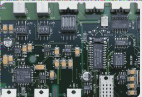
+ Real Picture Result (Via Coverage with Solder Mask)

As shown in the images above, you can see the clear distinction between vias covered with a solder mask and those that are not. This process ensures a higher-quality and more reliable PCB design.
If you have any further questions or need clarification on PCB design or assembly (PCBA), feel free to reach out to me at info@wellcircuits.com.