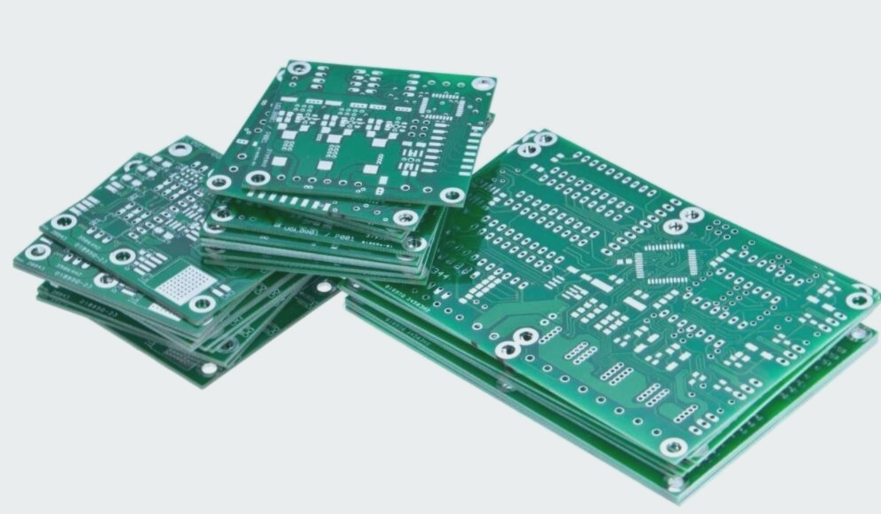
Common Challenges with PCB Parts Falling Off: Causes and Analysis
Many process and quality control engineers face concerns about PCB parts falling off, with issues ranging widely. Novices often struggle to identify where to start their analysis. Here, we will discuss methods and steps to address this common problem.
Root Causes of Components Falling Off:
- Issues with circuit board surface treatment
- Problems with component solder pads surface treatment
- Oxidation due to inadequate storage conditions
- Inconsistencies in the reflow temperature process
- Insufficient solder strength for external forces
Steps for Analyzing PCB Component Failure:
When dealing with falling components on a circuit board, the following steps are crucial:
- Gather Information: Confirm details about the incident, including conditions, testing, and environment.
- Identify Timing and Location of Issue: Determine if the problem occurs during production or on the client side.
- Examine Surface Treatments: Check the board’s treatment (ENIG, OSP, HASL) and component leads.
- Evaluate Board Thickness: Consider how thickness affects deformation and tin cracking risks.
- Assess Solder Paste Composition: Note differences in solder paste compositions and melting points.
- Acquire Defective Products: Collect faulty PCBs and fallen components for analysis.
- Check Solderability: Evaluate solder presence on pads and component leads using a microscope.
- Troubleshoot Soldering Issues: Look for defects like de-wetting or rejection caused by poor treatment or storage conditions.
- Request Supplier Inspection: If oxidation is suspected, involve the PCB supplier for analysis.
- Consider Disputes: Resolve conflicts by measuring surface treatment thicknesses or resorting to slicing for detailed analysis.
- Evaluate Component Solderability: Use a microscope to identify subtle solderability issues.
By following these steps and considering the root causes, engineers can effectively analyze and troubleshoot PCB parts falling off, leading to improved quality control and production processes.

Determining Tin Quality on Component Leads
When assessing the tin quality on component leads, it’s crucial to examine the plating layer composition in relation to the reflow furnace temperature. Components with silver plating should be noted for their surface layer nature, making them vulnerable to SAC solder paste, potentially impacting soldering strength.
Checking for Copper Exposure
Some components may reveal copper at their cut surfaces, usually uncoated. While this area typically does not require tin, it’s strategically placed in non-critical positions.
Inspecting Solder Pads
The fifth step involves verifying if the solder pads detach along with the dropped component leads. If there are no solderability issues with the PCB or component leads, assessing the detachment of the PCB pads confirms the quality of soldering, indicating successful reflow.
Addressing Reflow Concerns
If the pads remain intact, evaluating whether the reflow temperature curve aligns with solder paste specifications is essential. In cases of excessive defects, attempting to resolder dropped components can help identify potential temperature or solder paste adjustments to rectify issues.
Examining Component Detachment
Examining the area where the component fell involves scrutinizing the PCB and component leads’ surface under a microscope. A rough surface may suggest sudden external forces, while a smooth surface could indicate failure due to prolonged vibration, particularly in ENIG PCBs with black nickel concerns.
Conducting Biopsy for Analysis
If previous steps do not pinpoint the cause of component detachment, conducting a biopsy to examine Intermetallic Compounds (IMC) and perform Energy Dispersive X-ray (EDX) analysis becomes necessary. Destructive slicing of both the PCB and dropped components aids in this analysis.
Purpose of Slicing
- Checking IMC generation, uniformity, and composition using EDX to assess solder strength and component stability.
- Identifying fracture points to determine if issues lie within the solder strength or the PCB/component ends, guiding potential enhancements like Underfill for improved stability.
Extended Reading:
Exploring the relationship between PCB soldering strength and Intermetallic Compounds (IMC).


 العربية
 简体中文
简体中文 Nederlands
 English
 Français
 Deutsch
 Italiano
 日本語
日本語 한국어
한국어 Português
 Русский
 Español
 ไทย
ไทย