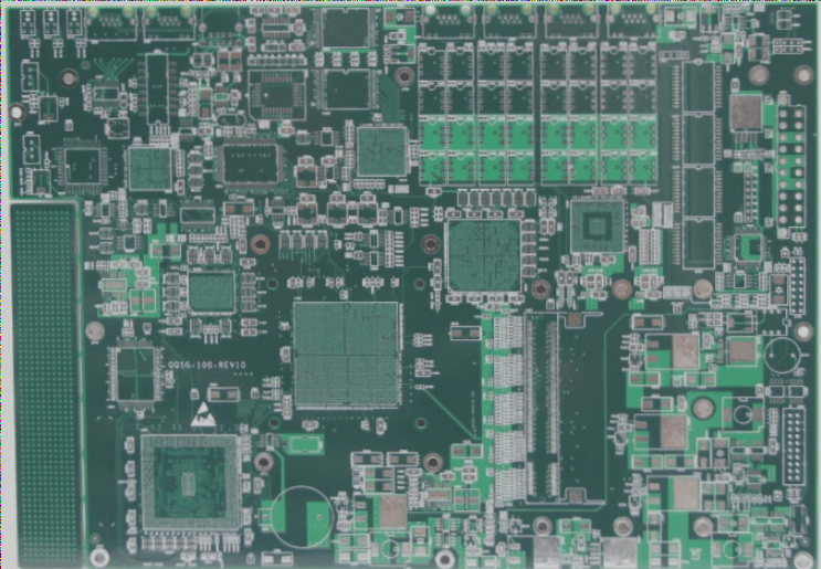
PCB Design: Enhancing Circuit Performance and Reliability
PCB design, or Printed Circuit Board design, is the process of translating a circuit schematic into a physical layout that meets specific functional and performance requirements. The primary goal is to ensure the PCB satisfies electrical, thermal, and mechanical constraints while optimizing manufacturability and reducing production costs.
Key Elements of PCB Design:
- Component Layout: Optimal placement of components for signal integrity, manufacturing ease, and space efficiency.
- Connection Layout: Proper routing of traces, vias, and interconnections to minimize signal loss and interference.
- EMI Protection: Employing strategies like ground planes and shielding to reduce electromagnetic interference.
- Thermal Management: Ensuring proper heat dissipation to prevent damage and maintain performance.
Recent developments in PCB design focus on advanced CAD tools for intricate designs, improving efficiency and accuracy.
Benefits of a Well-Designed PCB Layout:
An optimized layout enhances signal integrity, reduces noise, and improves heat dissipation, leading to overall cost savings during production.
PCB Design Process Steps:
- Component Placement: Categorize and place components to avoid interference and ensure proper grounding.
- Routing and Interconnection: Minimize noise and cross-talk while maintaining signal integrity.
- Thermal and EMI Considerations: Manage heat dissipation and minimize electromagnetic interference for reliability.
Guidelines for Optimal PCB Layout and Component Placement
When designing a PCB, the board size significantly impacts design efficiency. Considerations like PCB size influence signal integrity, cost, and device performance. Here’s a structured approach to PCB design, emphasizing component placement, layout techniques, and design considerations.
The Importance of PCB Design
The first crucial step in PCB design is determining the optimal size of the board. If the PCB is too large, it can lead to increased impedance, reduced signal integrity, and higher production costs. Conversely, if it is too small, heat dissipation becomes challenging, and the risk of signal interference rises. Once the PCB size is finalized, the strategic placement of special components is essential.
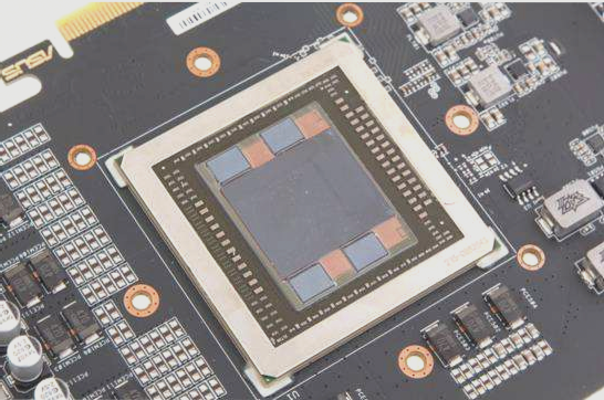
Principles for Special Component Layout
- Minimize High-Frequency Interference: High-frequency components require minimizing trace length to reduce impedance and electromagnetic interference. Components susceptible to interference should be spaced far apart, with inputs and outputs positioned at opposite ends of the board.
- High Voltage Components: Components operating at high voltages must be spaced adequately to prevent accidental shorts caused by discharge, keeping them away from other components.
- Heavy and Heat-Generating Components: Components over 15g should be secured with brackets for stability, placed on the bottom plate of the enclosure for thermal management, and away from sensitive components to prevent overheating.
- Adjustable Components: Components like potentiometers and micro switches should be easily accessible for adjustment, with a balanced layout to avoid top-heavy areas.
Success in design relies on functional placement and achieving a balance between quality and aesthetics.
Component Placement Order
- Structural Components: Start with components related to the board’s structural design, such as power connectors and switches.
- Special Components: Place large, heavy, or heat-generating parts like transformers and ICs after structural components.
- Small Components: Finally, position smaller components like resistors and capacitors, ensuring they do not interfere with larger parts.
PCB Layout Checklist
- PCB Size Consistency: Confirm that the PCB size matches the specified dimensions.
- Balanced Component Layout: Ensure even distribution and neat arrangement of components.
- Avoid Conflicts: Check for layout conflicts between components and printing levels.
- Accessibility of Commonly Used Components: Place switches and connectors in easily accessible locations.
- Thermal Considerations: Keep thermal components away from heat-sensitive parts.
- Heat Dissipation: Verify adequate heat dissipation paths on the PCB.
- Signal Interference: Address potential interference between traces, especially in high-speed circuits.
PCB Design Techniques and Best Practices
Grid Settings for Component Placement
During layout, precise component positioning is crucial:
- For large components, a grid accuracy of 50 to 100 mils is recommended.
- For smaller passive components, a finer grid setting of around 25 mils balances alignment precision and layout aesthetics.
PCB Layout Guidelines
- Component Placement on Same Layer: Place all components on the same layer, reserving the bottom layer for smaller components if the top layer becomes crowded.
PCB Layout Best Practices
- Grid-Based Arrangement: Components should be placed on the PCB using a grid system, either parallel or perpendicular to each other, for a neat and organized layout.
- Minimum Pad-to-Pad Distance: Maintain a minimum distance of 1mm between adjacent pads to prevent short circuits and manufacturing defects.
- Edge Clearance: Keep a distance of at least 2mm between components and the PCB edge, considering mechanical strength for larger PCBs.
Functional Circuit Unit Placement
- Signal Flow: Organize functional units based on signal flow to optimize signal propagation and reduce trace length.
- Centralized Core Components: Place core components at the center of each functional unit and surround them with peripheral components for efficient trace routing.
- High-Frequency Circuits: Pay attention to component distribution for high-frequency circuits, placing components in parallel to minimize signal reflections.
By following these principles and employing systematic layout techniques, PCB designs can achieve both functionality and aesthetic appeal. Proper component placement, thermal management considerations, and adherence to layout best practices ensure reliable performance in the intended application.