Creating SMD Footprints: A Step-by-Step Guide
In the previous tutorial, we covered how to create SMD pads for the 0603 footprint in Cadence Allegro. Now, let’s delve into the process of creating a footprint, using the 0603 footprint as our reference.
Footprint Specifications:
- Component: GRM033Z71C104KE14D from Murata Electronics
- Footprint Name: C0603
- Drawing Type: Package Symbol
Step-by-Step Instructions:
Step 1: Launch PCB Editor
Begin by opening the PCB Editor and selecting Allegro PCB Librarian XL.
Step 2: Create a New Footprint
In the menu bar, click “File” > “New” to create a new footprint. Enter the footprint name (C0603) and select “Package Symbol” as the drawing type.
Step 3: Set Design Parameters
Go to “Setup” > “Design Parameter” and adjust the User units to Millimeters for precision.
Step 4: Customize Grid Settings
Under “Setup” > “Grid”, modify the default grid from 2.54mm to 0.1mm for accurate placement.
Step 5: Define User References
Access “Setup” > “User References” to set the path for saving pads. Ensure proper configuration by clicking “Apply” and then “OK”.
Step 6: Add Pins
Under “Layout” > “Pins”, use the Options sidebar to add pads to the footprint.
Step 7: Finalize Placement
Place the pad by entering the coordinates in the command bar, followed by a right-click and selection of “Done” to complete the process.
By following these steps, you can effectively create an SMD footprint, tailored to your specific requirements.
Placing Pin Instructions for PCB Design
The process of placing pins on a PCB is crucial for proper circuit functionality. Below are the steps to follow:
Step 1: Placing Pin 1
To start, carefully position pin 1 on the designated spot. Refer to the image below for guidance:
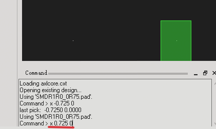
Step 2: Placing Pin 2
Once pin 1 is secured, proceed to place pin 2 accurately. Use the image reference for assistance:

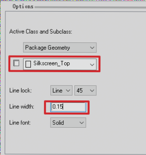
Step 3: Adding Silkscreen Outline
Enhance the PCB design by adding a silkscreen outline. Follow these steps:
- Click “Add” and select “Line” to define the layer and line width.
- Choose “Package Geometry” > “Silkscreen_Top” in the Options menu.
- Set the silkscreen line width to 0.15mm for precision.
Observe the visual representation of the completed silkscreen drawing below:
Mastering the pin placement and silkscreen outlining is fundamental in creating a well-executed PCB layout. Ensure accuracy and attention to detail for optimal results.