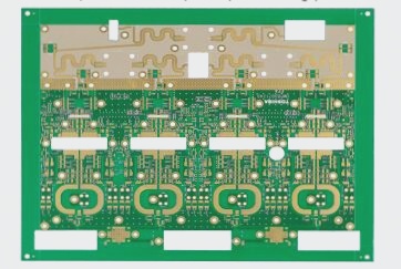
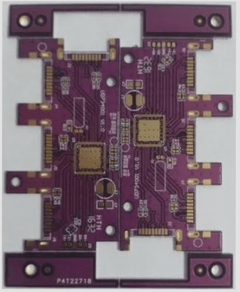
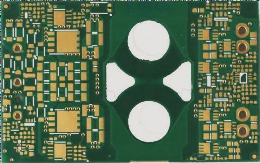
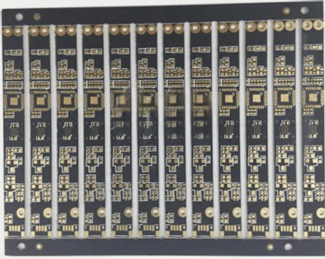
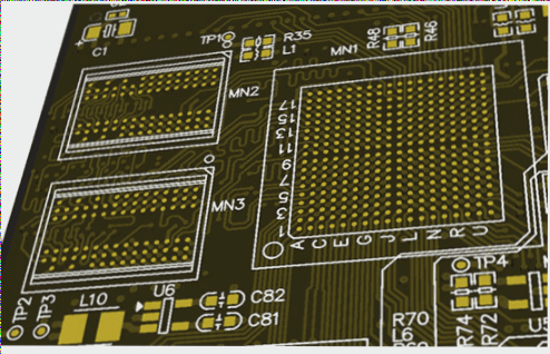
To create a PCB board is to transform a well-designed PCB schematic into an actual, functioning circuit board. Don’t underestimate this process. While many designs work in theory, they can be challenging to implement in practice, and what some can achieve, others may not. Therefore, making a PCB board is not inherently difficult, but designing a high-quality PCB is far from easy.
The two main challenges in the field of microelectronics are handling high-frequency signals and weak signals. In this context, the quality of PCB manufacturing becomes critically important. Even with the same design, components, and schematic, PCBs produced by different manufacturers can yield varying results. So, how can we ensure the creation of a high-quality PCB? Based on our experience, I would like to share my thoughts on the following aspects:
1. **Clarify the Design Objectives**
When receiving a design task, the first step is to clearly define the design goals. Is it an ordinary PCB, a high-frequency PCB, a small-signal processing PCB, or one that combines both high-frequency and small-signal processing? For an ordinary PCB, as long as the layout and routing are reasonable and organized, and mechanical dimensions are accurate, the task is relatively simple. If there are medium-load or long signal traces, specific measures should be taken to reduce the load, strengthen the long traces to ensure proper driving, and minimize issues such as signal reflections from long traces.
When signal lines on the board exceed 40MHz, special attention must be given to these high-frequency signals, including managing potential crosstalk between traces. For even higher frequencies, stricter limitations on trace length apply. According to distributed parameter network theory, the interaction between high-speed circuits and their traces plays a critical role and cannot be ignored in the system design. As gate transmission speeds increase, signal attenuation and interference on signal lines also grow, leading to increased crosstalk between adjacent traces. Additionally, high-speed circuits often require considerable power and generate significant heat, meaning special attention must be paid when designing high-speed PCBs.
When dealing with weak signals in the millivolt or microvolt range, the design requires even more care. These weak signals are highly susceptible to interference from stronger signals and typically need shielding to maintain signal integrity. Without proper shielding, the signal-to-noise ratio is severely degraded, and the useful signal can be overwhelmed by noise, making it difficult to extract valuable data.
1. **Consideration of Board Commissioning during the Design Stage**
The commissioning of the board should be taken into account during the design phase. The physical placement of test points, their isolation, and other related factors should not be overlooked, as small and high-frequency signals cannot always be measured directly with a probe.
Additionally, other important factors must be considered, such as the number of layers in the board, the packaging type of components, and the mechanical strength of the board. Before proceeding with the PCB fabrication, it is crucial to have a clear understanding of the design objectives.
2. **Understanding Layout and Routing Requirements for Components**
Certain components have specific layout and routing requirements. For example, the analog signal amplifiers used in LOTI and APH demand a stable power supply with minimal ripple. It is important to keep the analog signal section as far away as possible from power components. On the OTI board, the small signal amplification section is equipped with a shielding cover to protect against stray electromagnetic interference. The GLINK chip used on the NTOI board employs ECL technology, which consumes a significant amount of power and generates heat. Therefore, special consideration must be given to heat dissipation in the layout. If natural heat dissipation is used, the GLINK chip should be positioned in an area with good airflow, ensuring that its heat radiation does not affect other components. When the board includes high-power devices like speakers, the power supply may be significantly impacted, and this must be carefully addressed.
3. **Considerations for Component Layout**
The primary consideration when placing components on the board is electrical performance. Components that are closely connected should be placed near each other, particularly high-speed circuits. Power and small signal components should be placed separately and the trace lengths for high-speed signals should be kept as short as possible. While meeting circuit performance requirements, components should also be arranged neatly, with consideration for easy testing. The mechanical dimensions of the board and the placement of connectors must also be carefully planned.
Grounding and signal transmission delay times on high-speed systems should be a top priority in system design. The transmission delay on signal lines has a significant impact on overall system speed, especially for high-speed ECL circuits. While the integrated circuit itself may operate very quickly, the use of ordinary interconnects on the backplane (where a 30cm trace introduces a 2ns delay) can significantly increase transmission delay, slowing down the system. Synchronous components, such as shift registers and counters, should ideally be placed on the same board. Clock signal delays between boards can cause synchronization issues, potentially leading to errors in the shift register operation. If it’s not possible to place components on a single board, the length of the clock trace from the common clock source to each board must be identical to maintain synchronization.
4. **Considerations for Routing**
As the design of OTNI and the star optical fiber network progresses, there will be an increasing number of boards with high-speed signal traces above 100 MHz. Here, some basic concepts of high-speed signal routing are introduced.
**Transmission Line:**
Any “long” signal trace on a PCB can be treated as a transmission line. If the transmission delay of the line is much shorter than the signal rise time, the reflections that occur during the rise time will be suppressed. Overshoot, ringing, and recoil will no longer be an issue. For most MOS circuits in use today, the ratio of rise time to line delay is large enough that traces can be meters long without signal distortion. However, for faster circuits, especially ultra-high-speed ECL, trace length must be minimized to maintain signal integrity due to the increased edge speed of the integrated circuits. Without proper measures, longer traces can distort signals.
If you have any PCB manufacturing needs, please do not hesitate to contact me.Contact me