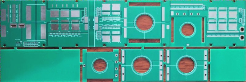
The Essential Steps in PCB Design
Designing a circuit board involves three crucial steps: circuit schematic design, netlist generation, and printed circuit board design. Adhering to specific requirements is essential for the device layout and wiring.
Key Considerations for PCB Design
- Input and Output Wiring: Minimize to prevent interference.
- Signal Line Routing: Separate parallel lines with a ground wire to reduce parasitic coupling.
- Layer Wiring: Wiring between layers should be perpendicular to mitigate coupling.
- Power and Ground Wires: Distribute across two layers with perpendicular orientation.
- Line Width: Use a broad ground wire as a loop for the digital circuit PCB.
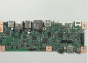
Principles for Microcontroller Control Boards
The article highlights important principles for PCB design in microcontroller control boards:
1. Component Layout
- Position related components closely, especially noise-sensitive ones like the clock generator and CPU clock input.
- Keep noise-generating circuits away from logic control circuits for improved reliability.
2. Decoupling Capacitors

- Install decoupling capacitors near critical components like ROM and RAM to reduce inductance effects.
- Place a 0.1uF decoupling capacitor between VCC and ground to mitigate noise spikes.
- Use ceramic capacitors for low ESL and high-frequency impedance.
3. Ground Wire Design
- Separate logic ground and analog ground paths to enhance interference immunity.
- Ensure the ground wire forms a closed loop for better anti-interference capacity.
- Use thick ground wires to stabilize signal levels and reduce interference.
PCB Layout Tips for Optimal Performance
- Carefully select grounding points
- Maximize trace width and alignment
- Optimize data line width
- Reduce vias for improved performance
For signal frequencies below 1MHz, opt for a single-point ground to reduce loops. For frequencies above 10MHz, use multi-point grounding to lower ground impedance due to significant PCB layout inductance.
When designing PCB layouts, maximize trace width based on current size. Align power and ground lines with data lines to enhance interference resistance. Use ground wires to cover trace-free areas on the board.
Widen data lines to minimize impedance, with a minimum width of 0.3mm (12mil) and an ideal range of 0.46-0.5mm (18mil-20mil).
Vias introduce capacitance and can lead to interference in high-frequency circuits. Minimize via usage during PCB design to maintain signal integrity and mechanical strength.
New PCB Layout Trends
Recent advancements in PCB design focus on reducing electromagnetic interference by optimizing grounding techniques, trace widths, and via usage. By following these latest trends, engineers can enhance circuit performance and reliability in high-frequency applications.