In PCB design, before the actual routing begins, there are several critical steps to follow. The process can be summarized as follows:
1. **System Specifications**
Initially, it is essential to define the system specifications of the electronic device. This includes factors such as system functionality, cost limitations, size constraints, operating conditions, and other relevant parameters.
2. **System Functional Block Diagram**
The next step involves creating a functional block diagram of the system. It is crucial to clearly indicate the relationships and interconnections between the different blocks in the diagram.
3. **Divide the System into Multiple PCBs**
If the system is broken down into multiple PCBs, it not only reduces the overall size but also provides flexibility for system upgrades and component replacement. The functional block diagram serves as the foundation for this partitioning. For example, in a computer, the system can be divided into several PCBs, such as the motherboard, graphics card, sound card, floppy disk drive, power supply, etc.
4. **Select Packaging Methods and Determine PCB Sizes**
The next step is to decide on the packaging methods for the components and finalize the size of each individual PCB.

**When the technology and number of circuits required for each PCB are determined, the next step is to define the board size. If the design becomes too large, packaging technology may need to be altered or redefined. When selecting a technology, the quality and speed of the circuit design must also be considered.**
**5. Create the circuit overview for all PCBs**
The outline drawing should detail the interconnections between components. Every PCB in the system must be traced. Today, CAD (Computer-Aided Design) is typically used for this purpose.
**PCB Overview**
The simulation of the preliminary design ensures that the circuit diagram will function properly. This must be simulated using computer software, which can read the overview and display the circuit’s operation in various ways. This approach is far more efficient than producing a physical PCB prototype and manually measuring its performance.
**Place the components on the PCB**
Component placement depends on how the parts are interconnected. They must be placed in a way that ensures the shortest and most efficient connections. Efficient routing means minimizing wire length and reducing the number of layers (which in turn lowers the number of vias). This topic will be revisited during the actual routing process. The following illustrates how the bus bar is routed on the PCB. Proper component placement is crucial for achieving optimal routing.
**Test wiring feasibility and high-speed operation**
Modern computer software can verify whether each component is positioned correctly for proper connectivity and if the design will function correctly under high-speed conditions. This step is referred to as “component arrangement,” but we won’t delve too deeply into it here. If issues arise with the circuit design, the components can be repositioned before the design is finalized.
**Export the circuit to the PCB**
At this stage, the connections shown in the overview diagram are translated into actual wiring on the PCB. This process is typically automated, though manual adjustments are often required. Below is an example of wiring for a two-layer board. The red and blue lines represent the component and solder layers of the PCB, respectively. The white text and squares indicate the screen printing layer markings. The red dots and circles represent drill and pilot holes. On the far right, gold fingers can be seen on the soldering surface of the PCB. The final layout of the PCB is typically referred to as “artwork.”
**Design regulations**
Every design must adhere to a set of standards, such as the minimum gap between traces, minimum trace width, and other practical design constraints. These standards vary depending on factors like circuit speed, signal strength, power consumption, noise sensitivity, and the quality of materials and manufacturing equipment. For example, if the current flow increases, the trace width must also increase. To minimize PCB costs while reducing the number of layers, it is essential to ensure compliance with these design constraints. If more than two layers are needed, power and ground layers are often added to protect the signal layers and prevent interference with signal transmission.
If you have any PCB manufacturing needs, please do not hesitate to contact me.Contact me
1. **System Specifications**
Initially, it is essential to define the system specifications of the electronic device. This includes factors such as system functionality, cost limitations, size constraints, operating conditions, and other relevant parameters.
2. **System Functional Block Diagram**
The next step involves creating a functional block diagram of the system. It is crucial to clearly indicate the relationships and interconnections between the different blocks in the diagram.
3. **Divide the System into Multiple PCBs**
If the system is broken down into multiple PCBs, it not only reduces the overall size but also provides flexibility for system upgrades and component replacement. The functional block diagram serves as the foundation for this partitioning. For example, in a computer, the system can be divided into several PCBs, such as the motherboard, graphics card, sound card, floppy disk drive, power supply, etc.
4. **Select Packaging Methods and Determine PCB Sizes**
The next step is to decide on the packaging methods for the components and finalize the size of each individual PCB.
**When the technology and number of circuits required for each PCB are determined, the next step is to define the board size. If the design becomes too large, packaging technology may need to be altered or redefined. When selecting a technology, the quality and speed of the circuit design must also be considered.**
**5. Create the circuit overview for all PCBs**
The outline drawing should detail the interconnections between components. Every PCB in the system must be traced. Today, CAD (Computer-Aided Design) is typically used for this purpose.
**PCB Overview**
The simulation of the preliminary design ensures that the circuit diagram will function properly. This must be simulated using computer software, which can read the overview and display the circuit’s operation in various ways. This approach is far more efficient than producing a physical PCB prototype and manually measuring its performance.
**Place the components on the PCB**
Component placement depends on how the parts are interconnected. They must be placed in a way that ensures the shortest and most efficient connections. Efficient routing means minimizing wire length and reducing the number of layers (which in turn lowers the number of vias). This topic will be revisited during the actual routing process. The following illustrates how the bus bar is routed on the PCB. Proper component placement is crucial for achieving optimal routing.
**Test wiring feasibility and high-speed operation**
Modern computer software can verify whether each component is positioned correctly for proper connectivity and if the design will function correctly under high-speed conditions. This step is referred to as “component arrangement,” but we won’t delve too deeply into it here. If issues arise with the circuit design, the components can be repositioned before the design is finalized.
**Export the circuit to the PCB**
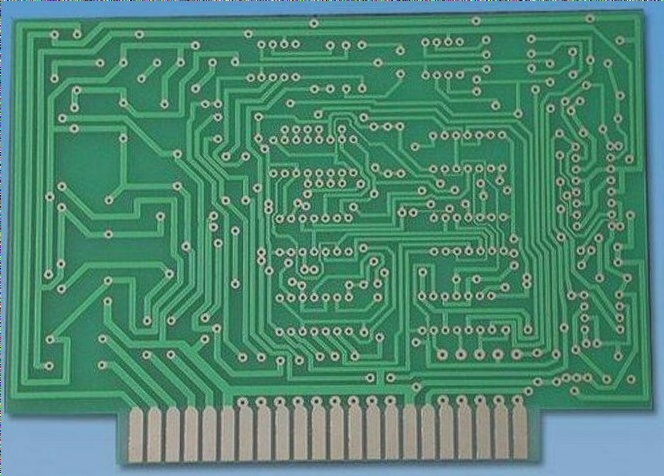
At this stage, the connections shown in the overview diagram are translated into actual wiring on the PCB. This process is typically automated, though manual adjustments are often required. Below is an example of wiring for a two-layer board. The red and blue lines represent the component and solder layers of the PCB, respectively. The white text and squares indicate the screen printing layer markings. The red dots and circles represent drill and pilot holes. On the far right, gold fingers can be seen on the soldering surface of the PCB. The final layout of the PCB is typically referred to as “artwork.”
**Design regulations**
Every design must adhere to a set of standards, such as the minimum gap between traces, minimum trace width, and other practical design constraints. These standards vary depending on factors like circuit speed, signal strength, power consumption, noise sensitivity, and the quality of materials and manufacturing equipment. For example, if the current flow increases, the trace width must also increase. To minimize PCB costs while reducing the number of layers, it is essential to ensure compliance with these design constraints. If more than two layers are needed, power and ground layers are often added to protect the signal layers and prevent interference with signal transmission.
If you have any PCB manufacturing needs, please do not hesitate to contact me.Contact me

