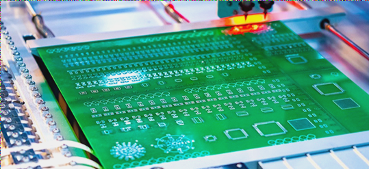
The Importance of Design Rule Checker (DRC) in PCB Design
Design Rule Checker (DRC) plays a crucial role in PCB design by identifying violations of design rules before the back-end processing begins. While schematic tools usually offer DRC functionality, they may not always be flexible enough for unique requirements.
Custom DRC for Specific Needs
Most tool vendors provide mechanisms for creating custom DRCs to better meet specific needs. This capability, although powerful, is not widely recognized or utilized. Custom DRCs can traverse the entire schematic diagram of the PCB design, generating valuable “by-products” that highlight subtle design rule violations.
Advantages of Custom DRC
A custom DRC can be easily updated to include new design features or attributes that impact design rules. By developing a custom DRC, users can also create tailored tools like a bill of materials (BOM) tool or a Verilog netlister to suit their unique requirements.
Programming with ViewDraw and ViewBase
Programming code examples for DRC can be done using tools like ViewDraw from Mentor Graphics and ViewBase, a library of C routines that interfaces with the ViewDraw database. These principles are applicable to any PCB schematic tools.
Input Files for DRC
In addition to the schematic database, DRC requires specific input files for handling various situations, such as legal power net names automatically connected to the power plane. These input files should be placed in a fixed global location for DRC to locate and read them at runtime.
Ensuring Correct Power Connections
Power/ground pins on component symbols are specified using attributes like SIGNAL = VCC or SIGNAL = GROUND. DRC reads these attributes to ensure that the network names match those in the input files. This verification is crucial to avoid critical errors in power connections.

Conclusion
Custom DRCs offer a flexible and powerful solution for ensuring design rule compliance in PCB designs. By leveraging the capabilities of custom DRCs, designers can address unique requirements and avoid costly errors in the design process.
Critical Considerations for PCB Design
When designing a PCB, it is crucial to pay attention to certain symbols that must include power/ground pins. These pins do not automatically connect to the standard power/ground plane. For instance, in an ECL device, the VCC pin might connect to VCC or GROUND, while the VEE pin could connect to GROUND or -5.0V. It is important to note that the power/ground pin can first connect to a filter before joining the power/ground plane.
Network Naming and DRC Verification
The network name between a pin and the filter can be arbitrary, as DRC does not verify this information. However, DRC may flag this as an error, prompting the user to either filter it out or add the net name to the ‘legal_pwr_net_name’ file, specifically for that design. This highlights the significance of files like ‘legal_pwr_net_name’ in PCB design.
Importance of ‘legal_pwr_net_name’ in DRC
Ultimately, ‘legal_pwr_net_name’ plays a crucial role in DRC by helping to: 1) identify the pull-up resistor, 2) verify the letter case of the POWER net name in the PCB design, and 3) identify any unused pins that are directly connected to POWER.


