Enhancing PCB Solder Resist Appearance Quality
Introduction
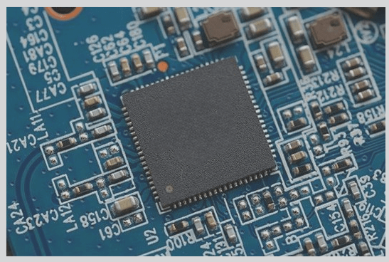
When discussing PCB development trends, precision, density, and reliability are often emphasized. However, the appearance of PCBs is gaining importance, with users demanding specific aesthetics. The solder resist, a crucial component of PCBs, must meet standards for thickness, hardness, solvent resistance, and adhesion. Additionally, it should have a uniform, glossy surface free from debris and marks. Enhancing the appearance quality of PCB solder resist is a vital challenge for manufacturers.
Factors Influencing PCB Solder Resist Appearance
Silk Screen:
Factors like squeegee flatness, printing environment cleanliness, and sealing tape type can impact the appearance quality of solder resist ink during screen printing. Uneven squeegees, workspace debris, and improper sealing tape can lead to surface imperfections.
Exposure:
Inadequate curing during the exposure process can result in imprints when the solder mask film adheres to the solder resist, affecting aesthetic quality.
Development:
Horizontal transfer development methods can damage the solder resist surface, creating roller marks. Improper exposure energy may impact gloss, but can be managed with a wedge meter.
Post-Curing:
Uneven temperatures during curing can cause inconsistent coloring, leading to yellowing or blackening, affecting visual quality.
Enhancing PCB Solder Resist Appearance
Silk Screen:
Regularly monitor squeegee conditions during ink printing to prevent surface marks. Conduct tests on tape and ink compatibility to avoid rubber particles on the surface.
Ink and Tape Compatibility Test Results:
- Tape A with Ink B: Best results, minimal rubber particles.
- Tape B with Ink A/B: Acceptable results, but Tape B is costlier.
Attention to ink and sealing tape compatibility is crucial to prevent surface imperfections in PCB solder resist production.
Key Strategies for Achieving High-Quality Aesthetic PCBs
Creating PCBs with high aesthetic appeal requires meticulous attention to detail throughout the production process. From silk screening to post-curing, every step plays a crucial role in ensuring the final product meets quality standards.
1. Clean Environment for Silk Screening
- Clean all surfaces in contact with the PCB using dust rollers.
- Designate transport vehicles for cleanroom use.
- Operators must wear specialized cleanroom attire and follow strict protocols.
- Maintain air purification and consider regular water spraying to reduce dust accumulation.
2. Addressing Negative Film Adhesion During Exposure
Preventing negative film adhesion during solder mask exposure is crucial for enhancing PCB aesthetics. Consider the following:
- Maintain glass plate temperature below 30°C during exposure.
- Optimize vacuum level to prevent film sticking.
- Use dedicated MYLAR film on the exposure frame and lithographic film for dry film exposure.
3. Mitigating Roller Marks During Development
Equipment adjustments can help prevent roller marks on the PCB solder resist during development:
- Use soft materials for transmission and pressure rollers.
- Ensure stability of the transmission system.
- Regularly clean pressure and squeeze rollers to avoid dirt buildup.
4. Uniform Post-Curing for Optimal Results
Post-curing plays a vital role in maintaining PCB quality:
- Regularly test oven temperature uniformity at multiple points.
- Establish guidelines for loading ovens and board orientation to prevent uneven heating.
Conclusion
Enhancing the aesthetic quality of PCB solder resist requires a holistic approach involving process optimization, equipment maintenance, and operator adherence to protocols. By monitoring and optimizing each stage of production, PCBs can achieve visual excellence that exceeds customer expectations.