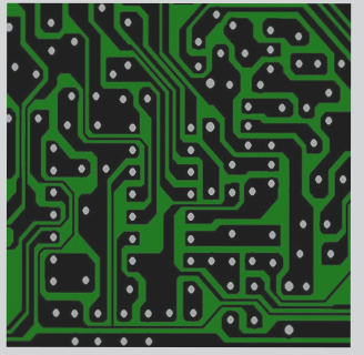
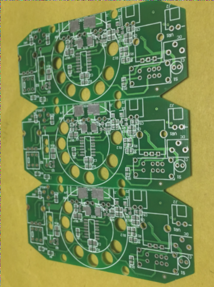
PCB Manufacturing Process: Importance of Electrical Testing
In the process of manufacturing PCBs, detecting defects early is crucial to minimize remediation costs. Thorough testing post-production is essential to ensure the functional quality and performance of the PCB. Without proper testing, the reliability and performance of the PCB cannot be guaranteed.
1. Electrical Testing in PCB Production
- Test Data Sources and Formats: Establishing data type and format compatibility with testing equipment.
- Test Conditions: Factors like voltage, current, insulation resistance, and connectivity.
- Equipment Manufacturing Methods: Selecting suitable techniques and equipment for testing.
- Test Specifications: Detailed testing protocols and repair guidelines documentation.
Electrical testing is crucial at three key stages:
- After Inner Layer Etching
- After Outer Layer Etching
- Final Product Testing
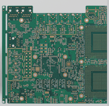
2. Electrical Testing Methods and Equipment
- Automated Optical Inspection (AOI): Detect visual defects and component alignment.
- Flying Probe Test: Uses probe needles to test electrical connections.
- In-Circuit Testing (ICT): Tests for short circuits, open circuits, and component values.
- Boundary Scan Testing: Detects faults in high-density boards.
These methods help in early defect detection and quality assurance of PCBs.
Primary Electrical Test Methods for PCBs
Key testing methods include specialized testing, general-purpose testing, and flying probe testing. Specialized testing offers high accuracy for specific designs but lacks flexibility. General-purpose testing is flexible and suitable for high-density testing. Flying probe testing uses probe needles for contactless testing.
Flying Probe Testing in PCB Manufacturing
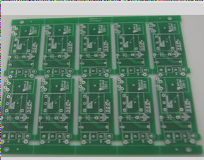
Flying probe testing is a minimalistic approach in PCB manufacturing that utilizes two probes moving across the X, Y, and Z axes to test individual circuit endpoints. Unlike specialized testing, flying probe testing does not need custom fixtures, making it cost-effective during setup. However, this method has slower testing speeds as each test point is probed individually. It is best suited for small-volume production, prototypes, and sample testing but is inefficient for medium- to high-volume production due to its slower pace.
Technology Comparison
Flying probe testing is ideal for small-volume production and PCB prototypes due to its flexibility and lower initial costs. However, its slow testing speed and relatively high equipment costs make it less suitable for medium-to-large scale production. On the other hand, general-purpose and specialized testing methods become more cost-effective with increased production volumes, benefiting from economies of scale. The cost of testing can drop to as low as 2-4% of the selling price once PCB production reaches a certain volume.
With the rapid pace of PCB innovation leading to shorter product life cycles and more frequent design changes, new technologies such as electron beam (E-Beam) testing, conductive epoxy molding (CEM), and plasma discharge testing are emerging as potential alternatives. While these methods are still in development, enhancements in test efficiency could position them as strong contenders for high-speed and high-accuracy electrical testing in the future.
Conclusion
The choice of PCB testing method depends on factors like production volume, cost considerations, and required testing speed. Specialized and general-purpose tests are suitable for larger production runs, whereas flying probe testing remains the top choice for small-batch or prototype PCB testing. Emerging technologies like E-Beam and CEM hold promise for enhancing test efficiency in the future.