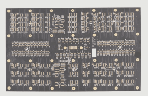
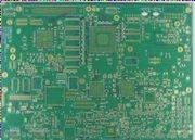
Routing a High-Quality Differential Pair on a PCB Copy Board
Factors Influencing Transmission Line Impedance
- Line width, length, and thickness
- Sidewall profile and resistive layer coverage
- Dielectric constant and thickness
Understanding these factors is crucial for achieving controlled impedance in differential pair routing. By adjusting line parameters, you can ensure fixed impedance for the transmission line.
Parallel Wiring and Differential Pair Advantages
- Implement parallel wiring for signal lines
- Advantages of using a PCB copy board for differential lines
Differential routing reduces external interference and maintains signal stability by ensuring equal length and impedance for differential lines.
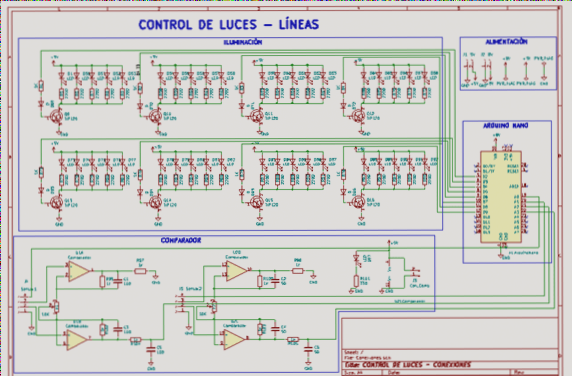
Differential Signal Design and Noise Reduction
- Differential signal marking in schematic design
- How differential lines reduce noise and EMI
Proper design considerations and differential pair routing techniques help eliminate noise and minimize electromagnetic interference.
PCB Routing Considerations and Connectivity
- Routing best practices for differential pairs
- Addressing connectivity issues for capacitive loads
Keep differential lines on the same layer, consider impedance matching, and pay attention to potential connectivity challenges for optimal PCB design.
PCB Copy Circuit Design: Tips for Terminal Impedance Matching
When working on PCB copy circuit design, it is crucial to focus on terminal impedance matching to prevent issues like reflection and EMI. Differential signal transmission primarily utilizes the differential mode, while considering the common mode can also be beneficial.
Reference Design for Terminal Impedance Matching
- Use an impedance analyzer to measure and calibrate the matching resistance.
- Common values for differential terminal resistance are 50 ohms or 100 ohms.
- Further fine-tuning may be necessary in practical applications.
- Differential mode signals are referenced to each other, not to ground, reducing common-mode RF energy.
- Initiate the PCB design model with the differential mode and make adjustments based on different mode testing during debugging.
If you have any inquiries regarding PCB design, feel free to reach out to us at info@wellcircuits.com.