Understanding Electronic Boards: Features and Repair
- Electronic boards, also known as printed circuit boards (PCBs), are crucial components in various technological devices, from aircraft control panels to TV remote controls.
- Damage to electronic boards can occur due to physical shock, oxidation, or moisture, necessitating electronic board repair.
- Each electronic board is unique, comprising plastic and fibrous materials with metallic tracks that conduct electric current.
- Proper repair of electronic boards is essential to ensure the correct functioning of associated equipment.
- Choosing experienced professionals for electronic board repair is crucial to avoid further damage to the system.
Steps to Repair a Damaged PCB
- Long-term oxidation of copper on PCBs can lead to corrosion, commonly caused by water exposure.
- Corrosion on unprotected PCBs or in humid environments can damage components like connectors and resistors.
- Visual diagnosis helps identify damaged areas and plan specific repair actions.
- Replacement of damaged elements like integrated circuits, capacitors, resistors, and terminal blocks is necessary for effective repair.
- Protective measures such as using Capton tape safeguard delicate components during repair processes.
Preparing for Soldering New Parts
- Reconstructed pads on the PCB are coated with gel flux, ready for soldering new components.
- Desoldering and soldering of damaged and new surface-mount device (SMD) components require precision tools like a low-power soldering iron and hot-air soldering station.
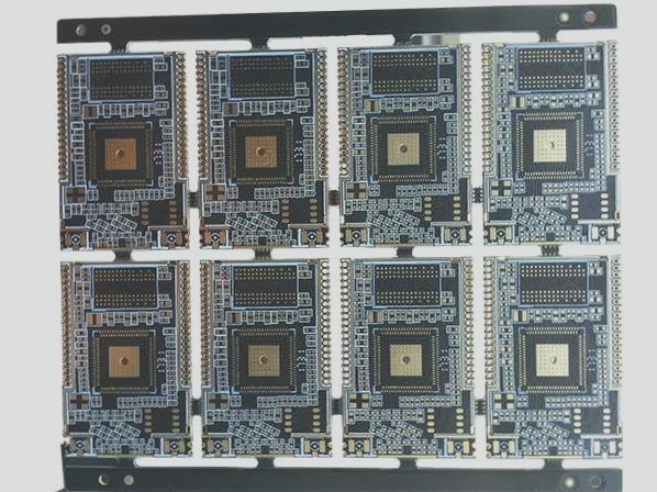
Check out the image below to see the PCB board:

Desoldering Terminal Blocks on a PCB: A Step-by-Step Guide
Desoldering a 6-pin terminal block on a PCB requires precision and the right tools. Using a heater soldering iron with a “screwdriver” tip and a Weller automatic suction device can make the process smoother. Additionally, a preheater with a temperature of around 200°C can help speed up the desoldering process.
It’s essential to maintain the process temperature below 440°C, especially when working with lead-free solder. For repairs, using tin with added lead at 325°C is recommended, aligning with the RoHS directive for electronics repair.
PCB Repair and Inspection: Post-Desoldering
After desoldering and soldering components, the PCB should undergo thorough inspection. The board should be cleaned, excess flux removed, and electrical connections checked. A new rail socket can be soldered in as needed before final testing.
Not all PCB damage is repairable or economically feasible. Some factors, like damaged components or vias on multi-layer panels, may disqualify a board from repair services.
Reasons a PCB May Not Qualify for Repair:
- Unidentifiable component damage
- Vias damage on multi-layer panels
- Broken path connections on inner layers
- Extensive damage due to fire or high temperatures
Understanding Insulation in PCB Boards
Adding thermal insulation material to a PCB can impact heat dissipation, potentially leading to overheating and component failure. Pollution events, like short circuits caused by contaminants, can also damage the board.
Regular cleaning and maintenance are crucial to prevent damage and ensure optimal device performance.
Protecting Your PCB: Cleaning and Maintenance Tips
Printed circuit boards are susceptible to dirt and debris accumulation, which can cause overheating and malfunction. Preventive measures, such as cleaning fan intake areas and avoiding liquid exposure, can help maintain PCB integrity.
Liquid contaminants, even in small amounts, can trigger short circuits and harm electronic devices. Proper cleaning techniques and safety precautions are essential for preserving PCB functionality.
Preventive Measures for Keeping Circuit Boards Clean
To prevent dirty boards and ensure the longevity of your electronics, it’s essential to take some preventive measures. One effective way is to always switch off any unused electronics, as this significantly reduces the risk of water damage. It allows the affected areas to dry out before further operation, minimizing potential adverse effects.
Handling Tips for Printed Circuit Boards:
- Always disconnect the device from the power source before handling
- Avoid working near water to prevent accidents
- Wear dry clothing to minimize the risk of static discharge
When disassembling equipment, be cautious as it can pose hazards to the electronics. Ensure you are familiar with proper handling techniques and reassembly procedures to maintain the devices’ functionality.
Effective Ways to Clean Circuit Boards
Proper PCB cleaning is crucial for maintaining optimal performance. Here are some recommended methods and tools:
- Utilize compressed air to remove dust and debris
- Consider using baking soda for gentle cleaning
- Isopropyl alcohol can be effective for removing stubborn contaminants
- Use distilled water for a final rinse
- Household detergents can also be used for thorough cleaning
When cleaning, remember to use a soft brush and a lint-free cloth to avoid damaging the components.
Summary: Maintaining Circuit Boards
When encountering failures in circuit boards, it’s crucial to focus on preventive measures to enhance fault tolerance and prevent future issues. Proper cleaning and maintenance play a significant role in extending the lifespan of electronic devices. By following the recommended cleaning methods and handling techniques, you can ensure the optimal performance and safety of your circuit boards.


