1. In PCB design, effective anti-ESD protection can be achieved through proper layering, strategic layout, and careful installation. By adjusting the PCB layout and routing, it is possible to significantly mitigate ESD risks. It is recommended to use multi-layer PCBs wherever possible. Compared to double-sided PCBs, multi-layer designs with dedicated ground and power planes, along with tightly spaced signal and ground traces, can reduce common-mode impedance and inductive coupling, achieving improvements of up to 1/10 to 1/100 of that found in double-sided designs. This setup ensures that components on both the top and bottom surfaces are interconnected with very short traces.
2. Static electricity from sources such as the human body, environmental factors, or even other electronic devices can cause severe damage to sensitive semiconductor chips. This can include penetrating the thin insulating layers within components, damaging the gates of MOSFET and CMOS devices, locking triggers in CMOS circuits, shorting reverse-biased PN junctions, short-circuiting forward-biased PN junctions, or even melting solder joints and aluminum wires inside active components. To prevent electrostatic discharge (ESD) from interfering with and damaging electronic devices, a range of protective measures must be employed.

In PCB design, anti-ESD measures can be achieved through careful layering, layout, and installation. Most design modifications can be predicted and limited to the addition or reduction of components. By optimizing PCB layout and routing, ESD can be effectively mitigated. Below are some common considerations.
1. Use multi-layer PCBs whenever possible. Compared to double-sided PCBs, multi-layer designs with dedicated ground and power planes, along with tightly spaced signal and ground lines, reduce common-mode impedance and inductive coupling. This results in a reduction of up to 1/10 to 1/100 compared to double-sided PCBs. Try to position each signal layer close to a power or ground layer. For high-density PCBs with components on both sides, short traces, and extensive fills, consider using inner-layer routing.
2. For double-sided PCBs, use a tightly interwoven power and ground grid. Keep the power plane close to the ground plane, and ensure numerous connections between vertical and horizontal traces, or filled areas. The grid size should be less than or equal to 60mm, with an ideal size under 13mm. Strive for compact circuit layouts.
3. Position connectors at the edges of the PCB as much as possible. If feasible, bring power lines in from the center of the board, avoiding areas most vulnerable to ESD.
4. On all PCB layers beneath connectors exposed to the exterior (which are more prone to ESD), place a broad chassis ground or polygon fill, connecting them with vias spaced approximately 13mm apart.
5. Place mounting holes along the edge of the PCB and ensure the top and bottom pads around these holes are free of solder resist, connecting directly to the chassis ground.
6. During assembly, avoid applying solder to the top or bottom pads. Use screws with built-in washers to ensure secure contact between the PCB and the metal chassis/shielding layer, or support on the ground plane.
7. Maintain an “isolation zone” between the chassis ground and the circuit ground on each layer. If possible, keep the separation at 0.64mm. On the top and bottom layers near mounting holes, connect the chassis ground and circuit ground with a 1.27mm-wide trace every 100mm. Adjacent to these connection points, add pads or mounting holes for attaching the chassis ground to the circuit ground. These connections can be isolated with a blade to keep the circuit open or bridged using magnetic beads or high-frequency capacitors.
8. If the PCB is not housed in a metal chassis or shielding device, avoid solder resist on the top and bottom chassis ground traces to allow them to function as discharge electrodes for ESD arcs.
2. Static electricity from sources such as the human body, environmental factors, or even other electronic devices can cause severe damage to sensitive semiconductor chips. This can include penetrating the thin insulating layers within components, damaging the gates of MOSFET and CMOS devices, locking triggers in CMOS circuits, shorting reverse-biased PN junctions, short-circuiting forward-biased PN junctions, or even melting solder joints and aluminum wires inside active components. To prevent electrostatic discharge (ESD) from interfering with and damaging electronic devices, a range of protective measures must be employed.
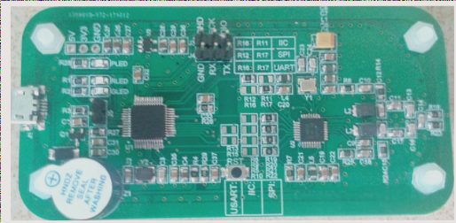
In PCB design, anti-ESD measures can be achieved through careful layering, layout, and installation. Most design modifications can be predicted and limited to the addition or reduction of components. By optimizing PCB layout and routing, ESD can be effectively mitigated. Below are some common considerations.
1. Use multi-layer PCBs whenever possible. Compared to double-sided PCBs, multi-layer designs with dedicated ground and power planes, along with tightly spaced signal and ground lines, reduce common-mode impedance and inductive coupling. This results in a reduction of up to 1/10 to 1/100 compared to double-sided PCBs. Try to position each signal layer close to a power or ground layer. For high-density PCBs with components on both sides, short traces, and extensive fills, consider using inner-layer routing.
2. For double-sided PCBs, use a tightly interwoven power and ground grid. Keep the power plane close to the ground plane, and ensure numerous connections between vertical and horizontal traces, or filled areas. The grid size should be less than or equal to 60mm, with an ideal size under 13mm. Strive for compact circuit layouts.
3. Position connectors at the edges of the PCB as much as possible. If feasible, bring power lines in from the center of the board, avoiding areas most vulnerable to ESD.
4. On all PCB layers beneath connectors exposed to the exterior (which are more prone to ESD), place a broad chassis ground or polygon fill, connecting them with vias spaced approximately 13mm apart.
5. Place mounting holes along the edge of the PCB and ensure the top and bottom pads around these holes are free of solder resist, connecting directly to the chassis ground.
6. During assembly, avoid applying solder to the top or bottom pads. Use screws with built-in washers to ensure secure contact between the PCB and the metal chassis/shielding layer, or support on the ground plane.
7. Maintain an “isolation zone” between the chassis ground and the circuit ground on each layer. If possible, keep the separation at 0.64mm. On the top and bottom layers near mounting holes, connect the chassis ground and circuit ground with a 1.27mm-wide trace every 100mm. Adjacent to these connection points, add pads or mounting holes for attaching the chassis ground to the circuit ground. These connections can be isolated with a blade to keep the circuit open or bridged using magnetic beads or high-frequency capacitors.
8. If the PCB is not housed in a metal chassis or shielding device, avoid solder resist on the top and bottom chassis ground traces to allow them to function as discharge electrodes for ESD arcs.

