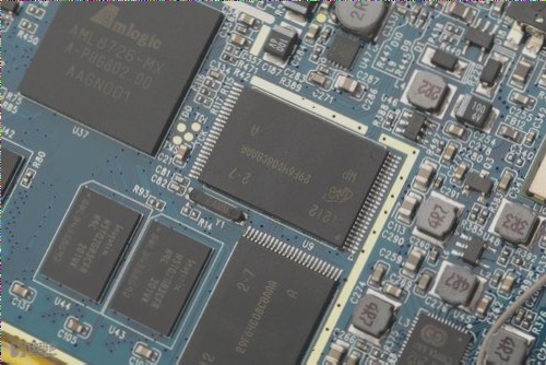
PCBs (Printed Circuit Boards) are essential in electronics, offering precision-engineered, rigid 2D designs crafted from fiberglass. These boards feature copper traces on the top and bottom layers, with copper-coated vias to allow electrical signals to pass through. A solder mask is applied to ensure solder stays precisely where it’s needed, while adding a functional color to the board. Lastly, a silkscreen layer allows for text and graphical elements to be printed on the board’s surface, making it both practical and visually informative.
However, designing a PCB can often feel like a monotonous and time-consuming task. After hours of reviewing layouts and schematics, the excitement of the project can begin to fade. It’s easy to become fatigued by the repetitive nature of the design process. So, how do you maintain enthusiasm and motivation throughout, so that when your boards arrive from Wellcircuits, you’re eager to assemble and test your creation?
One of the best ways to keep the design process enjoyable is to add creative touches to your board. While this list is far from exhaustive, here are a few of my favorite ideas to make your design more engaging:
First, consider incorporating custom text. Modern CAD tools like Altium, Eagle, and KiCad make it easy to add text to your design. But why stop there? Try placing the text on a copper layer instead of the usual silkscreen. The solder mask will darken slightly over the copper, allowing your text to remain subtle yet readable. For an even more eye-catching effect, create a solder mask keep-out area around the text, allowing the copper to shine through. Fun phrases or movie references can also add a personal touch to the design. One of my favorites is the line “I have spoken” from Disney’s *The Mandalorian*. Even if the text gets covered by components, knowing it’s there adds an element of fun.
Another approach is to get creative with the PCB traces. Unless you have specific impedance matching or signal integrity concerns, there’s no reason for traces to follow a straight, conventional path. Go ahead and experiment! Use the traces to create images or patterns. One of the most fun designs I’ve done featured Pac-Man chasing a series of small circles—all done with a single trace. Don’t be afraid to have fun with how you route your wires!
Moreover, consider breaking free from perfectly aligned components. For example, instead of placing all your SMD components in a strict, uniform orientation, try angling them slightly—say, at a 25-degree tilt. This small change adds a playful character to your board and gives it a less formal, more creative feel. If you’re feeling particularly adventurous, try rotating your connectors and ports to give the board a quirky, non-traditional look. Even something as simple as having a USB port not perfectly aligned with the edge of the board can add a fun touch.

Finally, challenge yourself by designing the smallest board possible. This goes beyond reducing the board’s overall footprint. Try to minimize material waste by pulling the board outline close to the traces and components. This can be tricky, so be sure to consult Wellcircuits’ manufacturing guidelines to ensure your design remains feasible. The result may be an oddly shaped board, but one that uses minimal fiberglass, making it both efficient and eco-friendly.

Whenever I start to feel fatigued with a design, I use these strategies to refresh my approach and reignite my passion for the project. By injecting creativity into the process, I stay excited about continuing the design and seeing my ideas come to life. Happy making!
If you have any questions about PCB design or PCBA manufacturing, feel free to reach out to me at info@wellcircuits.com.