Introduction:
There are various types of SMT (Surface Mount Technology) equipment. The design of the PCB must meet the specific requirements of the equipment, which depend on the type of machine. The following are the basic PCB design requirements for typical SMT equipment used in China.
Edge (Break-away Tab):
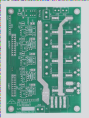
In the SMT process, PCBs are typically transported by rails. To ensure that the PCB is securely fixed during operations like pick-and-place or wave soldering, at least 5mm of space should be left on the edge of the transport track. This allows for proper rail engagement. If space cannot be reserved, a 5mm process edge should be added, as shown in Figure 1.

If the PCB design is not rectangular, a “Break-away tab” should be added to ensure two parallel sides. If this is not possible, clamps must be created during production to ensure the PCB can be properly positioned and transported through SMT equipment, as shown in Figure 2.

Tooling Hole:
SMT equipment such as printing presses and pick-and-place machines rely on positioning pins to align the PCB. Therefore, tooling holes must be included in the PCB design. Typically, two positioning holes should be placed at the ends of a rectangular PCB, with an aperture of 4mm.
For SMT equipment that transports PCBs from right to left, the left hole center should be positioned 5mm from both the left edge of the PCB, and the right hole center should be positioned 5mm from the bottom edge. The holes should be placed symmetrically around the PCB’s center of gravity, as shown in Figure 3. For machines transporting from left to right, the positioning is reversed.

Note:
Avoid placing any components within a 3mm radius around the tooling holes.
Products with functional PCBs that require online testing should also have a pair of tooling holes on the PCB’s diagonal. The aperture and spacing should be determined based on the testing equipment’s specifications. For non-rectangular PCBs, a break-away tab should be added similarly to a rectangular PCB.
Baseline:
To minimize positioning errors and PCB warping during mounting, most SMT equipment uses optical reference positioning. The baseline is typically defined by regular geometric shapes, usually consisting of dots or round holes with diameters of 0.8mm or 1.5mm. The baseline serves multiple purposes, including full-board alignment, component-level alignment for BGA and CSP components, and block alignment for daughter boards on motherboards.
Usually, two reference points are required as a pair, with a preferred diameter of 1mm. The reference points should be arranged diagonally on the PCB. The placement of these points should be as far apart as possible, ensuring that the rectangle formed by their diagonals can enclose all SMT components. Similarly, component and block baselines are also placed diagonally. Refer to Figure 4 for further details.

When the baseline point is a dot (highlight), a soldering zone must be designated where no soldering pads or wires are required. This zone should extend 1.5mm beyond the baseline point. When the baseline point is a round hole (dark point), a ring must be formed that is suitable for tinning, with a flat and shiny surface. This ring should also extend 1.5mm beyond the baseline point. The tin-plated area of the baseline point should be illuminated by the optical system, creating a high contrast with the surrounding area. This ensures better recognition of the baseline point after hot air reflow and uniform surface treatment.
The tin-plated area of the baseline points should show high contrast with the surrounding area when detected by an automatic optical inspection (AOI) system, after hot air reflow and uniform surface treatment. This contrast is critical for accurate baseline point recognition.
PCB Identification and Output Data:
To facilitate processing or meet the requirements of EMS (Electronics Manufacturing Services), the following identification and output data must be provided when the PCB design is transferred to the production department:
-
The PCB name, component positions and polarities, PCB markings, and production date.
-
Material list, PCB drawings, template files, assembly programming files, and other required documents. If testing is required, the schematic diagram and netlist are also needed.
-
Test conditions, standards, quality testing criteria, and specifications for post-soldering products.
-
Any additional requirements from the EMS provider.
Conclusion:
Standardized PCB design is essential for the systematic development of enterprises. It helps ensure the reliability, scalability, and quality of products, while contributing to cost reduction and increased efficiency. Businesses, as well as SMT (Surface Mount Technology) practitioners, must prioritize this aspect to improve product outcomes.
If you have any questions about PCB and PCBA, please contact me at info@wellcircuits.com