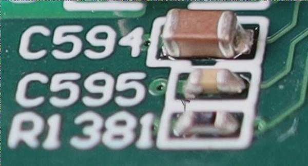
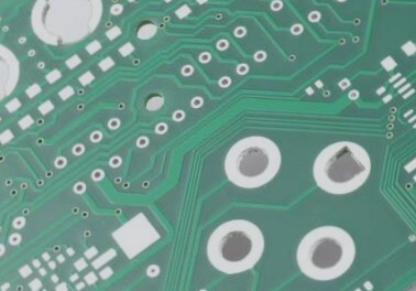
PCB Blind Vias: Enhancing Signal Integrity and Board Density
PCB blind vias are conductive holes that connect surface and inner layers without traversing the entire board. These vias, found on the top and bottom surfaces, link surface circuits with inner circuits below, improving signal integrity and reducing parasitic capacitance.
- Blind vias are common in High-Density Interconnect (HDI) PCBs, enabling designers to enhance signal integrity while minimizing PCB size.
- They offer new routing options and choices, eliminating the need for through-holes that pass through unconnected layers.
- Manufacturing blind vias involves processes like Sequential Lamination, Photo Defined, Controlled Depth, and Laser Drilled methods.
Advantages of PCB Blind Vias
- Reduce Signal Interference: Optimize signal transmission paths, ensure stability, and enhance product performance.
- Increase Board Density: Accommodate more components within the same PCB area, enhancing functionality.
- Improve Product Stability: Ensure stable signal reception and transmission, reducing failure rates.
PCB blind vias are essential for enhancing the performance and stability of electronic products, making them a crucial component in modern PCB design.