PCB design is advancing towards thinner, lighter, smaller, and higher-density integration. Rigid-Flex PCB, as an innovative combination of FPC and traditional rigid PCB, integrates flexible and rigid areas through lamination processes, showcasing unique advantages in space-saving and performance enhancement. Its three-dimensional structure is widely used in wearable devices, foldable screens, automotive electronics, and other fields, meeting the demands for miniaturization and high reliability.
WellCircuits Support 1-38 Layers Rigit Flex PCB Design and Manufacturing, Please see our product about RF PCB, if you have any RFQ about RF PCB, please feel free to contact us.
FCCL (Flexible Copper Clad Laminate)
Core Materials: Polyimide (PI) or Polyester (PET) film + Copper foil (Electrolytic copper foil/rolled copper foil).
Classification:
Adhesive FCCL: Copper foil is bonded to the substrate through an adhesive (such as epoxy resin), resulting in lower costs but with limitations in thickness and flexibility.
Adhesive-less FCCL: The copper foil is directly chemically bonded to the substrate, resulting in a thinner profile (e.g., 12.5μm) and greater flexibility, making it suitable for high-density designs such as foldable screens.
Common Types of Substrate Materials
Polyimide (PI)
Advantages: High temperature resistance (long-term 260°C, short-term 400°C), strong tear resistance, excellent electrical insulation, and high dimensional stability (moisture absorption rate 0.2-0.4%).
Disadvantages: Higher cost (accounting for 30-40% of FCCL cost), and attention must be paid to dimensional expansion after moisture absorption.
Applications: Mobile phone motherboards, automotive electronics, aerospace (e.g., Kapton® HN series).
Polyester (PET)
Advantages: Low cost (only 1/3-1/5 of PI), excellent flexibility, and superior water resistance.
Disadvantages: Poor high-temperature resistance (melting point 250°C, short-term temperature resistance 150°C), prone to shrinkage when heated (shrinkage rate 1-2%).
Applications: Consumer electronics (such as membrane switches), low-cost sensors.
- Coverlay Film (Coverlay)
Function: Protects circuits, insulates, and enhances mechanical strength.
Material Selection:
PI Cover Film: Compatible with the base material PI, resistant to high temperatures and corrosion, suitable for scenarios requiring long-term reliability.
Epoxy Resin (FR4) Coverlay: This has low cost but poor flexibility and high-temperature resistance; it is commonly used in rigid board areas.
Acrylic Adhesive: Excellent transparency, suitable for display modules (e.g., OLED screen connections).
Material Selection
PI Cover Film: Compatible with the base material PI, resistant to high temperatures and corrosion, suitable for scenarios requiring long-term reliability.
Epoxy Resin (FR4) Coverlay: This has low cost, but with poor flexibility and high-temperature resistance, it is commonly used in rigid board areas.
Acrylic Adhesive: Excellent transparency, suitable for display modules (e.g., OLED screen connections).
2. Material Classification and Characteristics
| Material Type | Thickness Range | Typical Application Scenarios | Advantages and Disadvantages |
| PI cover film | 12.7-127μm (1/2-5mil) | High temperature, high reliability scenarios (such as automotive electronics) | High temperature resistance (260°C) and strong chemical resistance, but it is costly (approximately 3-5 times that of epoxy resin). |
| Epoxy resin film | 25-50μm | Rigid board areas or low-cost products (such as membrane switches) | Low cost, but poor flexibility, with a long-term temperature resistance of ≤150°C. |
| Acrylic adhesive film | 10-25μm | Transparent display module (such as OLED screen connection) | It has excellent optical transparency but weak weather resistance and is prone to yellowing. |
3. Adhesive Selection
Thermosetting adhesives (such as epoxy resins): High temperature resistance, strong bonding strength, suitable for reflow soldering processes.Thermoplastic adhesives (such as polyester): Excellent flexibility but poor heat resistance (<120°C), commonly used for temporary protection.
2. Conductive Layer
1. Comparison of Copper Foil Types
| Type | Crystal Structure | Surface roughness | Adhesion | Typical thickness | Application Scenarios |
| Rolled Annealed Copper (RA Copper) | Smooth and dense | ≤1.5μm | Weaker | 9-35μm | High-frequency circuits and high-reliability products (such as 5G antennas) |
| Electrolytic copper (ED copper) | Rough and porous | ≥3μm | Stronger | 12-70μm | Ordinary flexible circuits (such as FPC cables) |
2. Alternative Materials
Silver sputtering/plating:
Process: Forming a silver layer through vacuum sputtering or screen printing.
Features: Excellent conductivity (conductivity ≈95% of copper), but high cost and poor corrosion resistance, commonly used in high-frequency devices (e.g., RF antennas).
3. Auxiliary Materials and Stiffeners
1. Reinforcement Material Selection
| Material | Characteristics | Application Scenarios |
| FR4 | High rigidity, low cost | Reinforcement of welding areas (e.g., BGA pads) |
| PI resin board | High temperature resistance, dimensional stability | Structural support in high-temperature environments (e.g., automotive ECU) |
| Metal sheet (steel/aluminum) | High thermal conductivity, high strength | Modules with high heat dissipation requirements (such as battery management systems) |
| Pressure-sensitive adhesive (PSA) | Temporary fixation, detachable | Test fixture or temporary assembly |
2. Design Considerations
Thickness Matching: The thickness of the reinforcement plate should transition gradually with the thickness of the flexible substrate to avoid stress concentration.
Heat dissipation design: Metal reinforcement should be used in conjunction with thermal conductive adhesive to prevent localized overheating, which could lead to material failure.
4. Low Flow Prepreg (Low Flow PP)
1. Key Parameters
| Model | Thickness (mil) | Resin Content | Flowability | Application Scenarios |
| 106 | 2 | 65% | Low flow | Ultra-thin rigid-flex board (≤0.4mm) |
| 1080 | 3.0-3.5 | 60% | Low to Medium Flow | Conventional rigid-flex boards (0.5-0.8mm) |
| 2116 | 5.6 | 55% | High flow | Thick board lamination or gap filling |
2. Process Function
Control interlayer bonding: Minimize adhesive overflow and prevent circuit contamination through low fluidity.
Dimensional stability: The resin shrinkage rate after curing is <1%, ensuring a flat bonding surface.
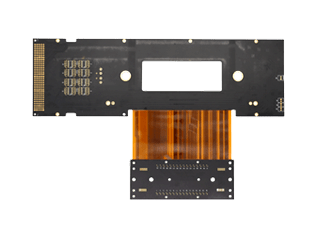
The structural form of a rigid-flex board.
A rigid-flex board is created by bonding one or more rigid layers onto a flexible board, enabling the circuits on the rigid layers to interconnect with those on the flexible layer through metallization. Each rigid-flex board features one or more rigid areas and a flexible area. Below is an illustration of a simple combination of rigid and flexible boards, with more than one layer.
Additionally, the combination of a flexible board with several rigid boards, or multiple flexible boards with several rigid boards, is achieved through drilling, plated through-holes, and lamination processes to establish electrical interconnections. This approach is tailored to the design requirements, making the conceptual design more suitable for device installation, debugging, and soldering operations. It ensures the optimal utilization of the advantages and flexibility of the rigid-flex boards. This scenario is relatively complex, involving more than two layers of conductive traces, as illustrated below:
Lamination is the process of pressing copper foil, prepreg sheets, flexible circuit layers, and outer rigid circuit layers into a multilayer board. The lamination of rigid-flex boards differs from that of purely flexible or rigid boards. It is essential to consider the deformation of the flexible board during lamination as well as the surface flatness of the rigid board. Therefore, in addition to material selection, the design process must account for the appropriate thickness of the rigid board to ensure that the expansion and contraction rates of the rigid and flexible parts are consistent, preventing warping. Experiments have shown that a thickness of 0.8 to 1.0 mm is most suitable. Additionally, it is important to place vias a certain distance away from the junction of the rigid and flexible boards to avoid affecting the rigid-flex interface.
1. Classification of Basic Structures for Rigid-Flex Boards
The rigid-flex board achieves functional integration through the lamination of rigid and flexible layers, with common structural forms as follows:
| Type | Structural Description | Typical Applications |
| Single-sided rigid-flex combination | A flexible layer is unilaterally laminated to a rigid layer (such as FCCL + FR4), connected through metallized vias. | Simple sensors, medical devices |
| Double-sided rigid-flex combination | Flexible layers are laminated with rigid layers on both sides, forming a symmetrical structure suitable for double-sided welding. | Mobile phone motherboard, tablet computer |
| Multilayer Rigid-Flex Combination | Flexible layers are alternately laminated with multiple rigid layers (such as FR4/PI/FR4), supporting complex circuits. | Automotive ECU, Avionics |
2. Complex Structural Combination Methods
Multi-flexible board + multi-rigid board combination
Structure Example: 2 Flexible Layers + 3 Rigid Layers (e.g., FCCL/FR4/FCCL/FR4).
Process challenges: Stepwise lamination is required to control the shrinkage rate differences between layers and prevent delamination.
Application Scenario: High-Density Packaging (e.g., Server Backplanes).
Three-dimensional structure
Technology: By pre-folding the flexible layer and then laminating the rigid layer, three-dimensional shapes such as L-shapes and U-shapes are formed.
Typical case: the hinge connection structure of foldable screen phones.
3.Lamination Process and Structural Design
Lamination Sequence Selection
First flexible, then rigid: first laminate the flexible layer, then overlay the rigid layer.
Advantages: Precise positioning of the flexible layer, suitable for ultra-thin structures.
First rigid, then flexible: first press the rigid layer, then laminate the flexible layer.
Advantages: The rigid layer provides support, reducing the risk of wrinkling.
4.Key Material Matching
Coefficient of Thermal Expansion (CTE): The rigid layer (FR4’s CTE≈18ppm/°C) and the flexible layer (PI’s CTE≈30ppm/°C) require stress buffering through low-flow adhesive PP.
Semi-cured sheet (PP): Select 106/1080 type low-flow PP to reduce adhesive overflow contamination on flexible circuits.
5.Key Points of Structural Design
Rigid area layout
Priority should be given to placing heavy components, such as BGAs and connectors, on the rigid layer to facilitate soldering and support.
The thickness of the rigid layer is recommended to be ≥0.4mm to ensure mechanical strength.
Flexible area transition design
Stepped transition: The edges of the rigid layer are tapered (such as beveled edges) to reduce stress concentration.
Rounded corner design: The corners of the flexible area are designed with an arc of R≥0.5 mm to prevent creasing and breakage.
Reinforcement plate application.
Reinforce the junction between the flexible layer and the rigid layer with PI or FR4 to prevent interlayer delamination.
Metal reinforcement requires reserved expansion space to prevent cracking caused by thermal stress.
Typical Structure Examples and Technical Parameters
| Structural Type | Number of Layers | Minimum line width/line spacing | Minimum Drill Hole Diameter | Application Areas |
| Single-sided rigid-flex | 2 layers | 75μm/75μm | 0.2mm | Consumer electronics (e.g., headphones) |
| Double-sided rigid-flex combination | 4 layers | 50μm/50μm | 0.15mm | Smartphone motherboard |
| Multilayer Rigid-Flex Combination | 6 layers | 35μm/35μm | 0.1mm | Automotive ADAS System |
| Three-dimensional structure | 8 layers | 25μm/25μm | 0.075mm | Foldable screen devices, wearable medical devices |
Production Process and Case Study Analysis of Rigid-Flex PCBs
I. Overview of the Production Process
The rigid-flex board integrates FPC and PCB processes, requiring synchronized control of manufacturing precision for both the flexible and rigid layers. The core processes are as follows:
Design and CAM Processing → FPC Manufacturing → Rigid Board Manufacturing → Lamination Bonding → Drilling and Metallization → Surface Treatment → Testing and Final Inspection
2. Detailed Explanation of Key Process Steps
1. Design and CAM Processing
Input files: Gerber files (including rigid layers, flexible layers, and laminated areas), IPC-2581 format data.
Process Planning:
Flexible Layer: Delineate the PI substrate area (e.g., 25μm thick), and mark the positions of IVHs (Interstitial Via Holes).
Rigid Layer: Determine the HDI structure (e.g., 0.5 mm BGA pitch), plan laser microvias (φ0.1 mm).
Lamination Control: Calculate the PP thickness (e.g., 106 type 2mil) to ensure the overall board thickness is 0.295±0.052mm.
2. FPC Manufacturing (using 25μm PI substrate as an example)
Steps:
PI Drilling: CO2 laser drilling of IVH holes (φ0.075mm), with a positioning accuracy of ±5μm.
Electroless Copper Plating: Deposit a 1-2μm copper layer to ensure uniform coverage on the hole walls.
Pattern Transfer: Dry film exposure and development to form 3/3 mil (76μm/76μm) circuits.
Etching and Stripping: Acidic etching solution (FeCl3) controls line width accuracy within ±10%.
Cover film lamination: PI cover film + thermosetting adhesive, cured at 180°C for 1 hour.
3. Rigid Board Manufacturing (FR4 Substrate)
Steps:
Laser Blind Via: UV laser drills a φ0.1mm hole with depth controlled to 1/3 of the board thickness.
Blackening treatment: Increase the roughness of the copper surface (Ra≥2.5μm) to enhance interlayer bonding strength.
Inner layer pattern: Dry film exposure forms 3/3mil circuit lines, with an etching precision of ±5%.
Lamination: Pre-lamination + vacuum pressing (180°C/30min), using 1080 type PP.
4. Lamination Bonding (Using 1+2F+1 Structure as an Example)
Craftsmanship:
Pre-alignment: Fiducial Mark visual alignment, accuracy ±10μm.
Vacuum Lamination:
Temperature: 180°C (below PI softening point)
Pressure: 3-5 MPa (to prevent wrinkling of the flexible layer)
Time: 45min (ensure complete curing of PP)
Cooling and Setting: Gradual temperature reduction (5°C/min) to minimize internal stress.
5. Drilling and Metallization
Steps:
Mechanical Drilling: φ0.2mm through-hole (rigid layer), using 0.1mm micro drill (flexible layer).
PTH (Electroless Copper Plating):
Activation treatment: Colloidal palladium catalysis ensures copper layer adhesion ≥1.5N/cm.
Full board electroplating: Current density 2-3 A/dm², depositing a copper layer of 25-35 μm.
Pattern Plating: Selectively thicken the copper in the holes to ≥30μm to meet the BGA pad requirements.
6. Surface Treatment
Rigid Area: ENIG (Electroless Nickel Immersion Gold), gold thickness 0.05-0.1μm.
Flexible Area: OSP (Organic Solderability Preservative), thickness ≤0.5μm, ensuring flexibility.
III. Representative Case: Motorola 1+2F+1 Mobile Display
1. Design Parameters
| Project | Requirements | Implementation Process |
| BGA pitch | 0.5mm | Laser blind vias (φ0.1mm) + micro via technology |
| BGA pitch | 0.5mm | Laser blind vias (φ0.1mm) + micro via technology |
| IVH Hole Design | Local interlayer conduction (e.g., between FPC layers) | CO2 laser drilling + selective electroless copper plating |
| Full board thickness | 0.295±0.052mm | Precisely control the PP thickness (Type 106,2mil). |
| Inner layer line width/line spacing | 3/3 mil (76μm/76μm) | Dry film photolithography + acid etching |
2. Technical Challenges and Solutions
Interlayer alignment accuracy:
Issue: Flexible layers are prone to stretching and deformation, leading to hole misalignment.
Solution: Utilize adhesive-free FCCL (such as DuPont Pyralux®), and pre-bake the PI substrate at 120°C for 2 hours before lamination to eliminate internal stress.
Ultra-thin board thickness control:
Issue: Avoid adhesive overflow from PP for a thickness of 0.295mm.
Solution: Utilize a vacuum laminator with segmented pressure control (initially apply 2MPa for pre-pressing, followed by 5MPa for pressure maintenance).
BGA Pad Reliability:
Issue: 0.5 mm spacing is prone to short circuits.
Plan: Utilize a negative dry film (such as Dupont Riston®), with the exposure energy optimized to 120-150mJ/cm², ensuring consistency in line width.
Via Location Design
- Core Rules
Dynamic Flex Area: Avoid placing vias in the flexible zone, especially in areas with dense BGA pads or high-frequency signal lines.
Safety Distance:
General application: The distance between vias and the edge of the rigid-flex junction area should be ≥50mil (1.27mm).
High reliability scenarios (e.g., automotive electronics): ≥70mil (1.78mm).
Processing Limit: Some manufacturers may accept ≥30mil (0.76mm), but prior confirmation is required. - Reinforced area processing
Holes are permitted in the flexible area covered by the reinforcement board (such as FR4), but they must be at least 20 mil (0.5 mm) away from the edge of the reinforcement board.
Example: Add PI reinforcement in the flexible area below the BGA pad, with the via located in the center region of the reinforcement.
Pad and Via Design
- Size and Shape Optimization
Pad Diameter: As large as possible while meeting electrical connection requirements (e.g., BGA pad diameter ≥0.3mm).
Transitional Design:
The connection between the pad and the trace should feature a 45° chamfer or an arc with a radius of R≥0.1mm to avoid stress concentration at right angles.Add pad teardrops with a width of ≥0.1mm to enhance mechanical strength. - Process Enhancement
Solder mask exposed copper ring: Diameter ≥ pad diameter + 2mil (0.05mm), facilitating soldering.
Via Teardrop: Add a teardrop (length ≥0.2mm) at the connection between the via and the trace to prevent via cracking.
Routing Design
- Interlayer layout
Avoid interlayer overlap: Traces on the same position in upper and lower layers must be staggered by at least 10 mil (0.25 mm) to prevent stress concentration during bending.
Cross-arrangement: Adjacent layers have perpendicular wiring directions (e.g., horizontal on the top layer and vertical on the bottom layer), reducing interlayer shear stress. - Path Optimization
Arc routing: Use arcs with R≥0.5 mm in the flexible area to avoid sharp corners (right angles can be retained in the rigid area).
Line width tapering: Use teardrop-shaped arcs at the transition between thick and thin lines (taper length ≥3 times the line width difference) to preven impedance discontinuity.
Copper Pour Design
- Structural Selection
Mesh copper foil: Suitable for high-frequency signals or scenarios requiring high flexibility, with a mesh spacing of ≥0.5 mm.
Solid copper sheet: Used for shielding or heat dissipation, but cutting slots (width ≥0.2mm) must be reserved in the bending area. - Optimization Recommendations
Fill non-functional areas (such as borders) with solid copper as much as possible to enhance overall rigidity.
Round the edges of the copper foil (R≥0.3mm) to reduce the risk of short circuits caused by burrs.
Spacing Between Drills and Copper Foil
- Drill to Copper
Minimum standard: ≥10 mil (0.25 mm), ensuring no gap between the hole wall and the copper foil during electroplating.
High reliability scenarios: ≥15mil (0.38mm), avoid electromigration in humid and hot environments. - Hole to Flex Edge
Recommended value: ≥50 mil (1.27 mm), to prevent delamination of the flexible layer due to drilling stress.
Rigid-Flex Junction Design
- Layer Stackup Layout
The flexible layer is situated in the middle of the layer stack, with the rigid layers symmetrically distributed (such as in a 1+2F+1 structure), reducing torque during bending. - Routing Rules
Direction perpendicular: The direction of the wire is perpendicular to the direction of bending (e.g., horizontal wiring corresponds to vertical bending).
Uniform Distribution: The spacing between conductors in the bending area should be ≥0.2mm to avoid localized concentration that could lead to breakage.
Maximum Line Width: Signal line width ≥0.1mm, power line width ≥0.3mm. - Via Restrictions
The use of PTH (Plated Through Hole) in the bonding area is prohibited; priority should be given to laser blind vias (such as IVH)
Bend Radius Design
- Calculation formula
Minimum bend radius (R) = Line width (W) × Plate thickness (T)
Single Layer:R ≥6T(T=0.1mm ,R≥0.6mm)。
Double Layer:R ≥12T(T=0.15mm ,R≥1.8mm)。
Muti Layer:R ≥24T(T=0.2mm ,R≥4.8mm)。 - Special Requirements
For high-frequency bending scenarios such as foldable screens: R ≥3mm, combined with UTG glass to enhance foldability.
Test Standard: Passed 100,000 cycle bend test (IPC-TM-6502.4.22F).
Design Reference Standards and Processing Capabilities
| Project | International Standard (IPC) | Domestic Processing Capability | International processing capability |
| Minimum line width/spacing | IPC-2223 3/3mil(76μm/76μm) | 75μm/75μm | 50μm/50μm |
| Maximum number of layers | IPC-D-249 Over 20 layers | 4 layers | More than 10 layers |
| Maximum number of layers | IPC-D-249 Over 20 layer | 4 layer | More than 10 layers |
| Interlayer Alignment Accuracy | ±75μm | ±100μm | ±50μm |
Design Verification and Reliability Testing
Simulation Analysis:
Perform thermal stress and mechanical bending simulations using ANSYS or ABAQUS to optimize the laminate structure.
Physical Testing:
Thermal Shock: -40°C to 125°C, 500 cycles (IPC-TM-6502.6.7).
Peel strength:≥1.5N/cm(IPC-TM-650 2.4.8)。
DFMEA:
Focus on analyzing the failure risks in the rigid-flex junction areas, BGA pads, and densely populated via regions.