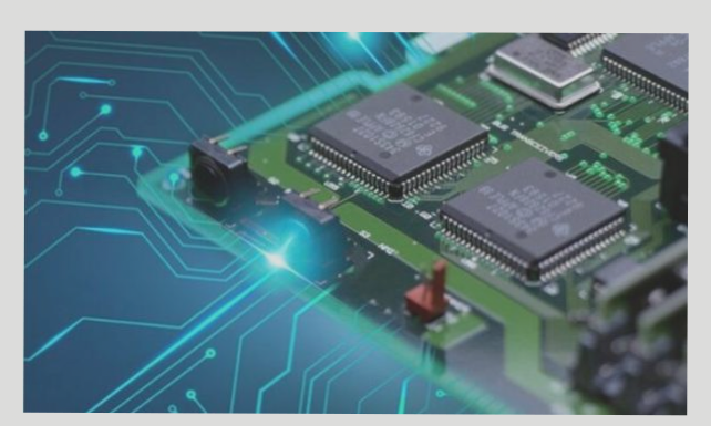
Common PCB Design Errors and How to Avoid Them
Printed circuit boards (PCBs) are essential components in various technologies, from computers to smartphones. As PCBs become more intricate, the likelihood of design errors increases. Here are some common mistakes and how to prevent them:
1. Layout Issues
- Missing Traces or Vias: Essential connections must not be overlooked.
- Incorrect Trace or Pad Size: Choosing the wrong size can lead to performance issues.
- Noise Generation: Poor grounding can result in signal integrity problems.
Solution: Use design rule checks (DRC) to ensure proper trace and pad sizes. Optimize signal routing for high-speed signals.
2. Schematic Errors
- Incorrect Component Placement: Misplacement can cause malfunctions.
- Connection Issues: Missing connections can lead to system failures.
- Inadequate Power Distribution: Ensure proper power delivery to prevent instability.
Solution: Review schematics thoroughly and use tools like electrical rule checkers (ERC) for validation.
3. Manufacturing and Testing Challenges
- Difficult-to-manufacture Designs: Complex layouts can pose fabrication challenges.
- Testing Complications: Small form factors may hinder testing processes.
Solution: Collaborate with manufacturers and consider design for test (DFT) principles for easier testing.
Conclusion
Advanced PCB designs come with increased error risks. By focusing on layout, schematic accuracy, and manufacturing feasibility, designers can create reliable boards. Automated tools and simulation software help ensure product integrity. Attention to detail and thorough verification are key to successful PCB development.
PCB Design Failures Due to Environmental Factors and Best Practices for Avoidance
1. Environmental Considerations in PCB Design: Environmental factors can impact PCB performance. Implement best practices to mitigate these effects.
Common Causes of PCB Failure and How to Prevent Them
- Environmental Factors: PCB failure can often be traced back to neglecting environmental considerations such as temperature, humidity, and vibration. Designers must account for these factors throughout the design process to ensure long-term reliability.
- Evaluation of EDA Tools: Choosing the right Electronic Design Automation (EDA) tools is crucial for efficient PCB design. Careful evaluation can improve layout efficiency and reduce errors, while the wrong tools can lead to design inaccuracies and manufacturing complications.
- Importance of Reviews: Regular reviews between PCB designers and electronic engineers are essential for aligning the final product with performance expectations. Effective collaboration can prevent operational failures and identify design flaws early on.
- Comprehensive Test Plan: A well-structured test plan is necessary to identify issues before full-scale production. Testing under various environmental stresses ensures the PCB’s performance under real-world conditions, preventing costly rework and product recalls.
- Handling Design Documents: Complete and organized design documents are crucial for smooth production. Incomplete files can lead to delays and errors, emphasizing the need for comprehensive, up-to-date documentation.
- Understanding Manufacturing Requirements: Designers must align their designs with manufacturing capabilities to avoid production issues. Awareness of material limitations and process requirements can reduce complexity and ensure timely and budget-friendly production.
- Avoiding Design Mistakes: Peer reviews help catch common design errors and inconsistencies. A fresh perspective can identify mistakes that the original designer might miss, ensuring a high-quality design.
- Leveraging Advanced Tools and Training: Utilizing advanced design tools requires comprehensive training to maximize their potential. Investing in learning these tools can lead to more precise designs, fewer errors, and faster iterations.
Integrating Design for Manufacturability (DFM) Tools
Improving PCB Design for Manufacturability
While layout design software has advanced, ensuring manufacturability is crucial. Designers should utilize Design for Manufacturability (DFM) tools to address potential manufacturing issues early on. These tools can detect problems like trace widths, hole sizes, or component placements that may complicate assembly, helping to avoid costly revisions and ensure smooth production runs.
Using Standardized Templates
Standardized design templates can streamline PCB design. By employing pre-defined templates that consider common design rules and manufacturing specifications, designers can maintain consistency, reduce the risk of missing crucial elements, and expedite the design process. Templates enhance accuracy, minimize errors, and ensure compliance with standards.
Collaboration with PCB Manufacturers
Building strong relationships with PCB manufacturers is key to enhancing the design and production process. Effective communication enables quick resolution of issues during design and manufacturing. Early collaboration helps identify and address problems, reducing the chances of delays or cost overruns. Maintaining good rapport with manufacturers ensures both manufacturability and cost-effectiveness of the PCB.
Avoiding Common PCB Design Pitfalls
Implementing these strategies helps designers steer clear of typical PCB design challenges. By considering environmental factors, using appropriate tools, and fostering transparent communication with manufacturers, designers can proactively create high-quality and reliable PCBs.
- If you have any inquiries about PCB or PCBA, don’t hesitate to contact me at info@wellcircuits.com.