It is well known that PCBs can easily bend or warp when passing through the reflow furnace. To help mitigate this issue, here are some helpful tips:

- Reduce the effect of temperature on PCB board stress
- Use high Tg material
- Increase the thickness of the PCB
- Reduce the size of the PCB and the number of panels
- Use reflow carriers/templates
- Use Router instead of V-Cut
Since temperature is the main cause of stress on the board, lowering the reflow furnace temperature or slowing down the heating and cooling rate can greatly reduce board bending and warping. However, this might introduce side effects such as solder short circuits.
The glass transition temperature (Tg) is the temperature at which the material transitions from a rigid glass state to a more flexible rubbery state. The lower the Tg value, the more quickly the board softens when passing through the reflow furnace, increasing the risk of deformation. Using higher Tg materials can improve resistance to deformation, though they tend to be more expensive.
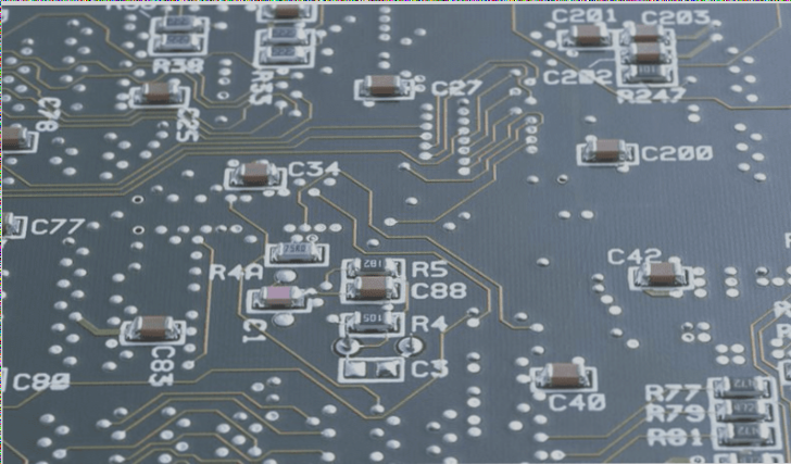
Many modern electronic products aim for thinner and lighter designs, with PCBs as thin as 0.6mm, 0.8mm, or 1.0mm. However, thinner boards are more prone to deformation during reflow soldering. If no thin or light requirement exists, it is recommended to use a board thickness of 1.6mm, which significantly reduces the risk of warping or bending.
As most reflow furnaces use chains to transport the boards, larger boards are more likely to deform under their own weight. Try to position the long side of the board parallel to the chain to minimize deformation. Additionally, reducing the number of panels in the furnace can further help minimize bending.
If the above methods are not feasible, a reflow carrier can be used to minimize deformation. The carrier helps stabilize the PCB during the heating and cooling process, preventing bending by fixing the board in place. Once the PCB’s temperature drops below its Tg value, the carrier helps maintain the original dimensions as it hardens.
If a single-layer carrier is insufficient to prevent PCB deformation, a two-layer carrier (clamping the PCB from both top and bottom) can be used for better results. However, note that using reflow carriers incurs additional tool and labor costs, as manual placement and removal are required.
V-Cutting weakens the structural integrity of the PCB panels, increasing the risk of deformation. It’s advisable to avoid using V-Cut or to reduce its depth if possible.
If you have any questions about PCBs or PCBA, feel free to contact us at info@wellcircuits.com.