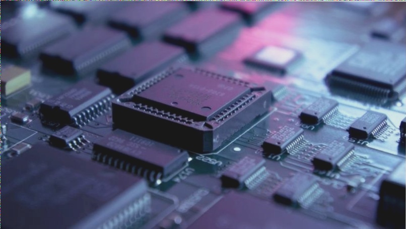
In the process of PCB duplication, a common dilemma arises. This occurs when temperature and humidity are inadequately controlled, or when the exposure machine overheats, leading to film deformation. The challenge is whether to proceed, risking quality and performance, or to discard the film, incurring cost losses. Here are some methods to rectify the deformed film.
1. Splicing method: This technique is suitable for negatives with inconsistent line patterns and varying degrees of deformation across layers, especially effective for correcting solder mask negatives and those of multi-layer power boards. The procedure involves cutting out the deformed sections of the negative film, re-splicing them according to the hole positions on a drill test board, and then proceeding with the duplication. This method works best for simple deformations with wide line widths and spacing, and irregular shapes, but is not suitable for negatives with high wire density or line widths and spacings under 0.2mm.
A gentle reminder: When splicing, take care to minimize damage to the traces and avoid harming the pads. When revising the layout post-splicing and duplication, ensure the connection relationships are accurate.
2. **Hole Position Adjustment Method**: This method is effective for correcting films with dense lines or uniform deformation across each layer. The specific process involves comparing the negative film with the drilling test board, measuring and recording the test board’s length and width, and then adjusting the hole positions on the digital programming instrument based on the measured deformations. This adjustment ensures that the drilled test board aligns with the deformed negative. The advantage of this method is that it eliminates the complex task of editing negatives, maintaining graphic integrity and accuracy. However, it may not effectively correct negatives with significant local deformation or uneven distortions.
**Note**: Mastery of the digital programming instrument is essential. After adjusting hole positions, reset any out-of-tolerance holes to maintain accuracy.
3. **Pad Overlap Method**: This method is suited for films with line widths and spacings greater than 0.30mm, where the pattern lines are not overly dense. The operation involves enlarging the holes on the test board to create overlapping circuit pieces with pads, ensuring compliance with minimum ring width technical requirements.
**Note**: After overlapping, the pads will appear elliptical, and the edges of the lines and pads may show halos and distortions. Users with strict aesthetic requirements for PCB appearance should apply this method cautiously.
4. **Photographic Method**: This method is applicable only for silver salt films and is useful when re-drilling the test board is impractical, provided the deformation ratios in both length and width are consistent. The operation is straightforward: use a camera to enlarge or reduce the deformed graphics.
**Note**: Film loss can be substantial, requiring multiple adjustments to achieve a satisfactory circuit pattern. Accurate focus is crucial during photography to avoid line deformation.
5. **Drying Method**: This method is suitable for undeformed negative films and can help prevent deformation post-copying. The process involves removing the negative film from its sealed bag before copying and hanging it in a controlled environment for 4–8 hours to allow for any deformation prior to copying. This significantly reduces the likelihood of further distortion after copying. Deformed films will require alternative measures.
**Note**: As environmental temperature and humidity affect film, ensure the conditions where the film is hung match those of the working area, and keep it in a well-ventilated, dark space to avoid contamination.
Ultimately, while the above methods serve as remedies for deformed films, PCB engineers should prioritize prevention. During the PCB copying process, maintain strict control of temperature at 22±2°C and humidity at 55%±5% RH. Utilize a cold light source or cooling device, and frequently replace backup films.