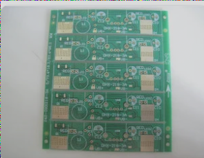
PCB Surface Treatment Methods: Choosing the Best Option
After completing the PCB design, selecting the right surface treatment process for the circuit board is crucial. Commonly used methods include HASL, ENIG, OSP, among others. The choice of surface treatment impacts costs and final results significantly.
1. HASL (Hot Air Solder Leveling)
The HASL process, available in lead-based and lead-free versions, was dominant in the 1980s but is less used now due to advancements in PCB technology. While lead-based HASL offers better mechanical strength and gloss, it contains harmful lead. Lead-free HASL is cost-effective and environmentally friendly, meeting standards like ROHS. However, its mechanical strength may not match that of lead-based HASL.
A common drawback of HASL PCBs is their unsuitability for soldering fine-pitch pins or small components due to poor surface flatness, potentially causing short circuits, especially with fine-pitch pin components during PCBA processing.
2. ENIG (Immersion Gold Technology)
ENIG is an advanced surface treatment ideal for circuit boards requiring functional connections and long shelf life. It offers resistance to oxidation, a long shelf life, flatness, and is suitable for soldering small-pitch pins and components with tiny solder joints. However, it comes at a relatively higher cost, and the welding strength may be weaker, leading to potential issues like “black pad” over time.
3. OSP (Anti-Oxidation Process)
The OSP process involves forming an organic film on bare copper surfaces, providing protection against oxidation, thermal shock, and moisture. While popular for various circuit boards, OSP is ideal when specific surface functionality or storage duration requirements are not a priority. It allows for easy bonding with molten solder, forming strong solder joints quickly.
OSP offers similar benefits to bare copper soldering, making it a preferred choice for resurfacing boards stored for up to three months, typically once.
Drawbacks of OSP Surface Treatment for PCBs
- OSP is prone to damage from acid and moisture exposure.
- Performance may decrease with each additional reflow soldering process.
- Boards must be reprocessed if stored for over three months.
- OSP must be used within 24 hours of opening.
- Extra steps are required to remove OSP for electrical testing due to its insulating properties.
- Significant process adjustments may be necessary for OSP application.
- Unprocessed copper can impact ICT testing results.
- Over-pointed ICT probes can damage the PCB, affecting test repeatability.
The comparison above highlights the differences in surface treatment methods for PCBs, including HASL, ENIG, and OSP. The selection of a surface treatment process should align with the specific requirements of the PCB’s intended use.
If you require PCB manufacturing services, feel free to reach out to me. Contact me