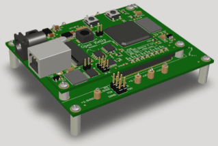
PCB Surface Treatment Methods: Choosing the Right Process
After completing the PCB design, selecting the appropriate surface treatment process for the circuit board is crucial. Commonly used methods include HASL (Hot Air Solder Leveling), ENIG (Electroless Nickel Immersion Gold), and OSP (Organic Solderability Preservative). The choice of surface treatment impacts costs and final results significantly.
HASL (Hot Air Solder Leveling)
The HASL process, available in lead-based and lead-free versions, was prevalent in the 1980s but is now less common due to advancements in PCB technology. While lead-based HASL offers better mechanical strength and gloss, it contains harmful lead. Lead-free HASL is cost-effective and environmentally friendly but may lack in mechanical strength and gloss.
- Advantages of lead-based HASL: Lower cost, excellent soldering performance.
- Disadvantages of lead-based HASL: Contains harmful lead, not environmentally friendly.
Common issues with HASL PCBs include poor surface flatness, making them unsuitable for soldering fine-pitch pins or small components.
ENIG (Immersion Gold Technology)
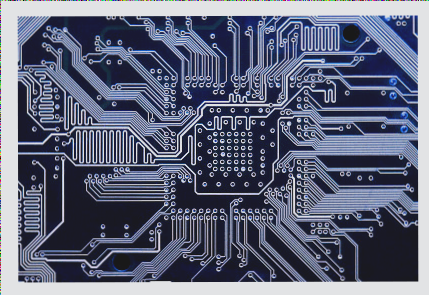
ENIG is an advanced surface treatment known for its resistance to oxidation and long shelf life. It is ideal for soldering small-pitch pins and components with tiny solder joints.
- Advantages of ENIG: Highly resistant to oxidation, long shelf life, ideal for small-pitch pins.
- Disadvantages of ENIG: Higher cost, weaker welding strength compared to other methods.
OSP (Anti-Oxidation Process)
The OSP process forms an organic film on bare copper surfaces, providing protection against oxidation, thermal shock, and moisture. It is popular for various circuit boards, offering benefits similar to bare copper soldering.
- Advantages of OSP: Protection against oxidation, suitable for various circuit boards.
When choosing a surface treatment method for your PCB, consider factors such as cost, environmental impact, soldering performance, and long-term reliability to ensure the best results for your specific application.
Challenges of OSP Surface Treatment
When it comes to OSP (Organic Solderability Preservative), there are certain drawbacks to consider:
- 1. Sensitivity to acid and humidity
- 2. Decreased performance with secondary reflow soldering
- 3. Time constraints for completing secondary reflow
- 4. Need for resurfacing if storage time exceeds three months
- 5. Limited usage window of 24 hours after opening
- 6. Requirement to remove OSP layer for electrical testing
- 7. Potential need for significant process changes
- 8. Negative impact on ICT testing if unprocessed copper is detected
- 9. Risk of PCB damage from over-pointed ICT probes
When comparing OSP with other surface treatment methods like HASL and ENIG, it’s essential to choose the right process based on the specific requirements of your PCB’s application.
If you are in need of PCB manufacturing services, feel free to reach out to us.