Optimizing PCB Heat Dissipation for High-Power Applications
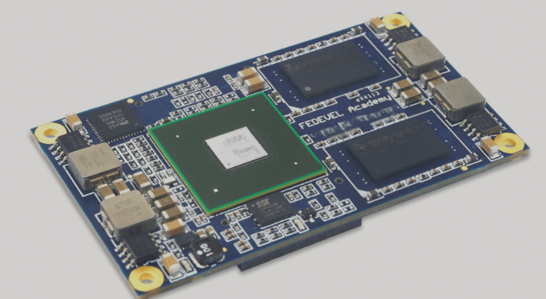
Surface mount IC substrate packaging relies on printed circuit boards (PCBs) for effective heat dissipation in high-power semiconductor devices. Proper PCB layout, structure, and device mounting are crucial for enhancing heat dissipation and system performance while reducing thermal risks.
Key Strategies for Heat Dissipation:
- Utilize wider traces on the top and bottom layers of the PCB to create efficient heat dissipation paths away from high-power devices.
- Incorporate dedicated heat spreaders positioned on the top or backside of the PCB to establish thermal links with devices through direct copper contact or thermal vias.
- Integrate metal reinforcement plates connected to the heat spreader to increase cooling surface area and enhance thermal performance.
Additional Cooling Solutions:
In larger PCB systems, consider connecting the heat spreader to the ground plane with screws to further enhance heat dissipation. While fans and heat sinks are common cooling solutions, they may require design modifications for optimal effectiveness in compact spaces.
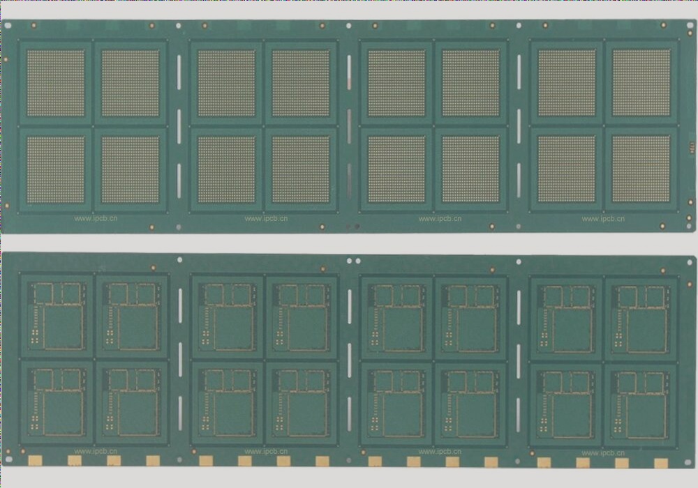
BGA IC Substrate Board Assembly:
When preparing BGA IC substrate boards, consider different positioning methods for accurate and efficient soldering:
- Line Drawing Positioning Method: Use a pen or needle to draw lines around the BGA-IC substrate board before removal for precise re-welding direction.
- Sticker Positioning Method: Affix label paper along the edges of the circuit board for easy reinstallation alignment post-removal.
- Visual Inspection Method: Position the IC carrier plate upright to ensure accurate alignment with the circuit board before installation.
These strategies and assembly methods aim to improve clarity and readability while emphasizing effective PCB heat dissipation and assembly processes.

Proper Method for BGA-IC Substrate Board Removal and Reattachment
When it comes to removing and reattaching a BGA-IC substrate board, following the correct procedure is crucial for successful results. Here are the steps to ensure a smooth process:
- Touch Method: Start by applying solder paste on the circuit board after removing the BGA-IC substrate board. Use an electric soldering iron to smooth each solder leg, creating rounded joints. Avoid flattening joints with a desoldering wick, as this can complicate the touch method.
- Alignment: Carefully maneuver the BGA-IC substrate board with solder balls across the circuit board. Pay attention to any resistance or movement, as these indicate alignment. If you see a circuit board pad around the edges of the IC substrate board, it means realignment is necessary.
- Soldering: Once aligned, solder the BGA-IC substrate board using a hot air rework station. Adjust the airflow and temperature to ensure even heating until the solder fuses and overflows. Avoid applying excessive pressure on the BGA-IC substrate board during heating to maintain proper alignment facilitated by the solder joints’ surface tension.
Latest Information:
Recent advancements in BGA-IC substrate board technology have led to the development of more efficient soldering techniques. Manufacturers are now focusing on improving the reflow soldering process to achieve higher yields and better reliability in electronic assemblies.


