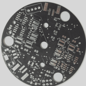
1. PCB patch technology is a widely adopted process in the electronics industry.

2. So, what exactly is a PCB? A PCB, or printed circuit board, is a crucial electronic component.

3. It serves as a foundation for interconnecting electronic components and electrical devices.

4. Simply put, any electronic device—from computers to our small electronic watches—that contains components like integrated circuits relies on PCBs to connect these various elements.

5. In the following sections, we will provide a detailed introduction to PCB boards.


1. The layers of a PCB primarily consist of the power layer, ground layer, and signal layer, with the total number of layers being the aggregate of each type. During the design process, the initial step involves coordinating and categorizing all power sources, grounds, and various signals, followed by deploying and designing based on this classification. Generally, different power supplies should be allocated to separate layers, and distinct grounds should correspond to their respective ground planes. Special signals, such as those with high clock rates or frequencies, must be designed with care, often necessitating an additional ground plane to shield these signals and enhance electromagnetic compatibility. When cost is also a consideration, it is essential to strike a balance between the system’s electromagnetic compatibility and its overall cost during the design phase.

2. The primary focus in designing the power layer is on the type and quantity of power supplies. If only a single power supply is used, a single power layer may suffice. For high power requirements, multiple power layers can be employed to supply power to devices across different layers. When multiple power supplies are present, one can opt for designing multiple power layers or distributing different power supplies across the same layer, provided that there is no crossover between them. In cases of crossover, separate power supply layers must be created.

3. The design of signal layers should reflect the characteristics of all signals involved. The layering and shielding of special signals is a crucial consideration in constrained designs. Typically, design software is initially used to create the layout, which is then refined according to specific details. Both signal density and the integrity of special signals are critical factors that must be addressed in layer design. For special signals, a ground plane layer should be incorporated as a shielding layer when necessary.

4. Generally, designing single or double-sided boards is not advisable unless cost is the sole consideration. Although single and double-sided boards are easier to manufacture and cost-effective, they may not be suitable for high signal density or complex signal structures, such as high-speed digital circuits or analog-digital mixed circuits. The absence of a dedicated reference ground layer in single-sided boards increases the loop area and radiation, while inadequate shielding diminishes the system’s immunity to interference.

5. The PCB serves as a vital substrate within the PCB assembly industry. It primarily comprises a power layer, a ground layer, and a signal layer. Typically, different power sources should be allocated to separate layers, and distinct grounds should have corresponding ground layers. Therefore, a key aspect of design is to establish proper layering, followed by subsequent deployment and design operations based on this structure.

Leave a Comment

Contact

WellCircuits
More than PCB

Upload your GerberFile(7z,rar,zip)