—
The automated printed circuit board (PCB) appearance inspection machine plays a crucial role in ensuring quality along the PCB production line. Utilizing optical image processing and computer vision recognition technology, its primary function is to detect appearance defects in PCB components during manufacturing. Despite China’s significant global PCB production volume, its position is not commensurate with its capacity. Weaknesses in PCB equipment and instrumentation are critical factors contributing to this scenario.
To advance China’s PCB industry, a manual PCB appearance inspection machine has been developed, offering simpler operation, a more compact system, and a higher performance-price ratio compared to automated systems. This manual machine employs a manual board transfer device to move PCBs, while a linear CCD camera scans them uniformly to capture precise images. Feedback signals automatically sort PCBs (OK/NG) based on detected defects, which include foreign objects, exposed copper, inadequate plating, scratches, incorrect markings, uneven solder mask, irregular pads, residual copper, missing prints, and other appearance flaws.
Given the direct impact of image acquisition and processing speed on PCB detection accuracy and efficiency, the image acquisition system is meticulously tailored for manual inspection machines. The development leverages the C# .NET framework for ActiveMil integration and utilizes the GDI+ graphics interface library to realize a robust image acquisition software system.
—
This revision maintains the technical details while enhancing clarity and readability.
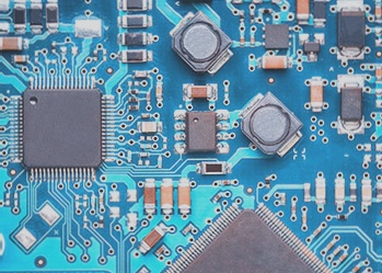
1. The overall structure of the PCB board appearance inspection machine system
The PCB board online detection system has a complex structure. Its transmission control equipment, electrical control system, and cameras must be computer-controlled to coordinate processing tasks and complete intricate detection and sorting operations. The system for PCB board online inspection based on machine vision is primarily divided into motion control, image acquisition, and image processing components. The image acquisition segment, akin to human eyes in machine vision, is pivotal for capturing object images and forms the foundation of detection processing. Emphasizing speed and accuracy, the PCB board inspection system necessitates the image acquisition part to deliver clear images promptly and precisely.
2. The hardware structure of the image acquisition system
2.1 The working principle of the image acquisition system
Upon system activation, the MCU automatically checks if the PCB stage has reset to the starting point. This process utilizes two fiber optic sensors and servo motors: one at the reset point and the other at the track endpoint. These sensors manage reset, halt, and motor reversal functions. Upon power-up, if the MCU detects an invalid signal from the reset point (sensor 1), it triggers the motor to reverse, returning the PCB stage to the starting position while sending an invalid color image signal to the PC via the serial port. Subsequently, the MCU monitors key presses; upon detection, the motor rotates forward, and a valid color image signal is sent to the PC. This sequence constitutes the PCB board line scanning process for image acquisition. During motor forward rotation, the MCU employs the capture and comparison unit (CCU6) to count pulses from the servo motor encoder. Upon reaching the required count for image acquisition, the serial port sends a start signal, initiating image capture by the linear array CCD as the motor decelerates toward sensor 2 at the track’s end. The motor halts and swiftly reverses to the starting point, prompting the serial port to send an invalid signal to the PC, thereby completing a full detection cycle. The MCU continues monitoring for subsequent down detection events. The CCD’s image signal is conveyed to the image acquisition card via the Camrelink interface for further processing by the PC.
2.2 Reception and detection of sensors and buttons
The use of optocoupler isolation technology facilitates optical-electrical isolation between circuits, ensuring smooth signal passage while mitigating spikes and noise interference. This approach enhances operational stability, longevity, and transmission efficiency without direct contact. For real-time feedback speed signal detection from the rotating mirror, the design integrates the high-speed optocoupler ACPL-072L. Operating at transmission rates up to 25 MBd, this component simplifies peripheral circuitry. Leveraging the XC164CS peripheral’s CC25 port and optocoupler-transmitted signals as external interrupt triggers, the XC164 achieves high-speed sensor positioning and button detection.
2.3 CCD camera system
The image acquisition system in this manual PCB board appearance inspection machine utilizes the NED Rainbow series 3CCD color line scan camera NUCLi7300. This camera supports diverse applications, enabling color difference detection previously unattainable with monochrome cameras. Featuring a high-speed Camera Link interface for seamless connectivity with capture cards, it supports easy gain and offset adjustments alongside RGB line delay correction. With 7,300 x 3 pixels and 10 x 10 μm pixel dimensions, it operates at a 60 MHz data rate and achieves a short scan rate of 7.6 kHz. The system’s frame acquisition card, Matrox SoliosXCL-SU74, boasts its processor for managing two independent base modes or one mid-mode Camera Link configuration. With a 66 MHz acquisition rate and 64 MB buffer, it accommodates area and line scan cameras across multiple acquisition modes. Despite prevalent use of area scanning cameras in most market image inspection systems, the PCB board appearance inspection machine’s wide product size range (50 mm x 50 mm to 330 mm x 250 mm) and demand for high precision and image acquisition speed necessitate the use of line scan CCD. Consequently, the acquisition card operates in hardware trigger synchronization mode for capturing and buffering 64 MB of memory.
3. Software system composition
The software for the image acquisition system is developed in C# using the AetiveMil 9.0 component. This platform integrates Matrox’s comprehensive package, the Image Processing and Pattern Recognition Library (MIL), and its sub-library MIL-LITE. MIL, a hardware-independent 32-bit image processing library, leverages Intel’s MMX multimedia graphics acceleration to optimize image processing across binary, grayscale, or color images, independent of hardware platforms. For expedited Windows application development, MIL bundles ActiveMIL, a dynamic control facilitating image acquisition, processing, analysis, display, and archiving. Integrated into Microsoft Visual Basic, Visual C++, and .NET environments, AetiveMIL streamlines programming, shortens development cycles, and enhances application stability. Utilizing AetiveMil control library, developers leverage MIL’s full functionality with ActiveX controls, reducing programming complexity and improving system stability.
3.1 Image acquisition program based on AetiveMil
The image acquisition program initializes by establishing a communication channel, configuring application and system objects for managing hardware resources such as data buffers, digitizers, and display units. Upon initializing the acquisition process, images are read into data cache, processed, and displayed. AetiveMIL’s integration with Windows UI simplifies application development through drag-and-drop interface design, significantly reducing code complexity. Following installation of the MIL development package and correct configuration in .NET Framework 3.0, essential components—Application, System, Image, ImageProcess, and Display—are automatically added to the toolbar, facilitating rapid application development.
3.2 The idea of double-buffer asynchronous acquisition
Matrox MeteorII frame grabber supports synchronous and asynchronous acquisition modes. Synchronous mode ensures continuous image acquisition and display without computational processing, necessitating CPU wait times between acquisitions. In contrast, asynchronous mode enables concurrent image acquisition and processing. Implementing a double-buffer mechanism buffers current and forthcoming image frames during acquisition, enhancing system efficiency and real-time processing capabilities. This method optimizes system resources, significantly boosting image acquisition speed and quality compared to traditional methods.
4. Image acquisition example
Implementing double-buffer asynchronous acquisition enhances image acquisition speed, reduces development cycles using ActiveX components, and lowers labor costs. Real-time, lossless stitching of 7,300 x 10,000 pixel images completes in just 1.3 seconds without frame drops, underscoring efficiency gains. Image buffer size calculation—MemSize = ImageWidth x ImageHeight x Frames—illustrates resource optimization. By comparison, synchronous acquisition of similar resolution demands approximately 6 GB of buffer space per frame, whereas asynchronous double-buffer acquisition requires less than 32 MB, demonstrating resource efficiency and superior acquisition performance.
5. Conclusion
Double-buffering technology, integrated with asynchronous acquisition, revolutionizes PCB board appearance inspection systems. Leveraging Matrox SoliosXCL-SU74, asynchronous double-buffer acquisition enables real-time, continuous image acquisition suitable for PCB boards (10 frames per second, 7,300 x 1,000 resolution). GDI+ library facilitates seamless, real-time, lossless image stitching, surpassing traditional methods in efficiency, hardware requirements, and suitability for large-scale image acquisition systems like PCB board appearance machines.

