Introduction to Integrated Passive Component Technology
As electronic technology advances, the demand for passive components to complement active electronic components is increasing. The trend in the electronic product market is towards lightweight and compact designs. However, the growing number of active components requires more space for passive components, leading to larger device footprints. Cost reduction and space efficiency have become crucial considerations in enhancing passive component performance.
Integrated Passive Component Technology
Integrated Passive Devices (IPD) technology integrates various electronic functions like sensors, RF transceivers, MEMS, and power amplifiers into compact products, enabling miniaturization and improved system performance. IPD technology plays a pivotal role in reducing product dimensions and weight or adding functionalities within existing product volumes.
Influence of IPD on PCB Board Technology
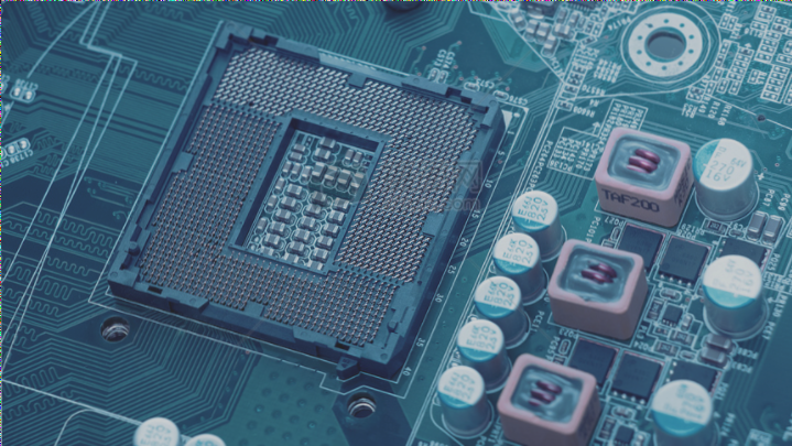
IPD technology has evolved to replace discrete passive components in industries such as ESD/EMI, RF, high-brightness LEDs, and digital hybrid circuits. It is integrated into PCB board processing to bridge the gap between packaging and PCB technologies.
Introduction to Thin Film IPD Technology
Thin film IPD technology, utilizing semiconductor processes, integrates circuits, capacitors, resistors, and inductors with high precision, repeatability, and cost-efficiency. It is positioned as the future mainstream IPD technology, offering compact size and reliability.
Development Status of Thin Film Integrated Passive Component Technology
Thin film IPD technology fabricates resistors, capacitors, inductors, and interconnecting transmission lines for passive components through processes like exposure, development, coating, diffusion, and etching. Manufacturers like Telephus use thick copper processes to enhance performance and reduce costs for passive components, benefiting wireless communication and integrated RF modules.
- Thick film processes like LTCC and HDI PCB technology
- Challenges and advantages of thin film IPD technology
- Manufacturing processes and precision in thin film IPD technology
Thin Film Integrated Passive Component Technology Overview
- IMEC’s thin film technology utilizes electroplated copper, BCB, and Ni/Au for interconnections and surface connections, with up to 4 metal layers.
- Dai Nippon’s IPD resistors use Ti/Cr, capacitors are anodized to Ta₂O₅, and inductors are designed with microstrip lines or spiral configurations.
- SyChip employs TaSi for resistors, Si₃N₄ for capacitors, Al for upper electrodes, and TaSi for lower electrodes, with aluminum for inductors and circuit materials. Some companies are exploring MEMS processes for IPD development.
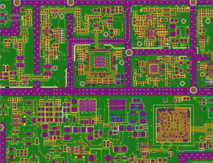
Structure and Process of Thin Film Integrated Passive Component Technology
Thin film processes differ from thick film primarily in film thickness, with thin film ranging from 0.01 μm to 1 μm. Integration of resistors, capacitors, and inductors into semiconductor manufacturing processes requires material compatibility and specific process design. Thin film IPD components can be produced on substrates like silicon wafers, alumina ceramics, or glass, utilizing processes such as lithography, thin film deposition, etching, and plating techniques. Active components can also be combined on silicon wafers to meet multifunctional requirements.
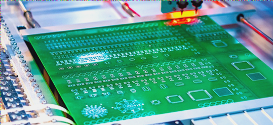
Thin Film Resistor Processing
Sputtering is used to deposit resistance materials onto insulating substrates, followed by photoresist and etching to create desired resistance patterns. Fabrication methods include vacuum evaporation, sputtering, thermal decomposition, and electroplating, considering temperature coefficient of resistance (TCR).
Film Capacitors
Film capacitors employ MIM structures for high-frequency applications, relying on dielectric material properties and substrate surface roughness to prevent electrode punctures.
Thin Film Inductor Processing
Design considerations aim to reduce parasitic capacitance and enhance component quality factor (Q). Electroplating is utilized for achieving required inductance wire thickness, with substrate surface roughness affecting high-frequency performance.
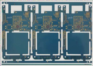
Impact of IPD Technology on PCB Board Development
PCB technology is evolving towards higher precision, density, and integration with IC packaging. IPD integrated passive components offer high wiring density, small size, and effectively integrate resistors, inductors, and capacitors for improved signal transmission and reduced costs, enhancing overall electronic system efficiency.
Conclusion
Thin film IPD technology enables miniaturization and enhanced system performance, replacing bulky discrete components and bridging the gap between packaging and PCB technologies. Its integration supports diverse applications in aerospace, medical, industrial control, and communications industries, enhancing PCB enterprise competitiveness and industry advancement.