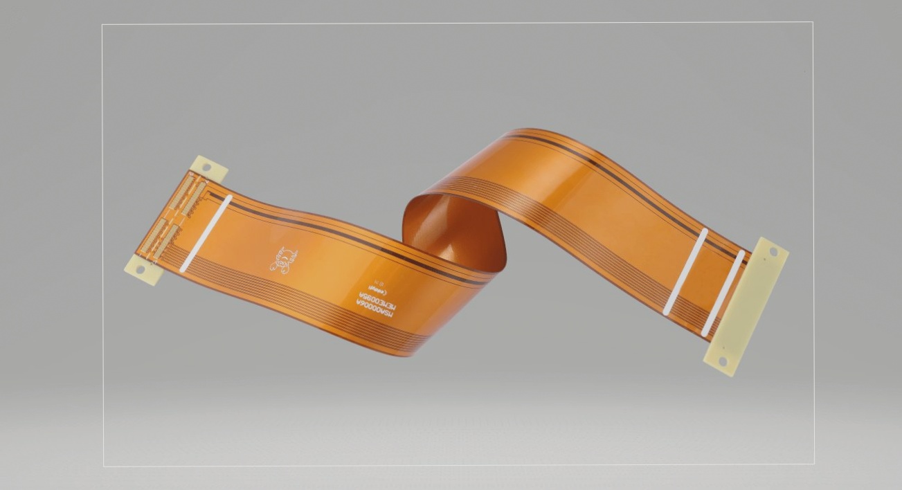
The Importance of Maintaining Continuous Impedance in PCB Design
Ensuring continuous impedance in PCB design is crucial for effective signal transmission. However, there are instances where impedance discontinuities may occur, leading to signal reflection and potential issues. Here are some key considerations:
1. Gradient Line
When dealing with small RF device packages, gradient lines are used to avoid sudden changes in line width. This helps prevent impedance disruptions. It is important to pay attention to the transition part of the line to maintain signal integrity.
2. Corner
Right-angle corners in RF signal lines can cause impedance discrepancies and signal reflection. To address this, chamfering or filleting the corners can help reduce impedance disruptions. A larger radius for the arc angle is recommended (R>3W).
3. Large Pad
Large pads on microstrip lines can introduce distributed capacitance, affecting the characteristic impedance. To mitigate this, thickening the microstrip line medium or hollowing out the ground plane under the pad can help reduce the impact of distributed capacitance.
4. Vias
Vias play a critical role in connecting transmission lines on different layers of a PCB. However, via stubs and parasitic parameters can lead to impedance issues. Utilizing a diskless process and optimizing the anti-pad diameter can help reduce via impedance discontinuities.
5. Through-Hole Coaxial Connector
Similar to vias, through-hole coaxial connectors can experience impedance disruptions. Implementing a diskless process, choosing a suitable lead-out method, and optimizing the anti-pad diameter on the PCB board can aid in minimizing impedance discrepancies.