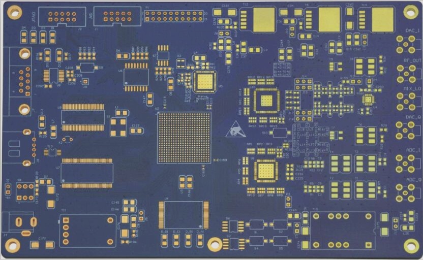
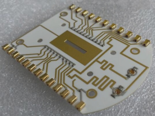
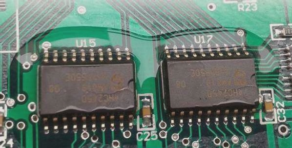
1. Rigid-flex PCBs are commonly populated with electronic components. When it comes to plugging, the conductivity and signal transmission performance need to be taken into consideration. Therefore, it is crucial that the impedance is kept as low as possible, with resistivity being less than 1/cm².
2. The technological process for rigid-flex PCB boards requires low resistivity to ensure that the overall impedance of the board meets the product quality requirements.
3. The conductors within the rigid-flex board will be responsible for various signal transmissions. When it comes to increasing the frequency in order to boost the transmission rate, any differences in the line itself due to factors such as etching, laminate thickness, wire width, etc., will result in a change in impedance, leading to signal distortion and reduced PCB performance. It is therefore essential to control the impedance value within a certain range.
Furthermore, it is not permissible to use the pads for soldering external assembly components as inspection points. Special test pads must be preset to ensure that solder joint inspection and production debugging can be carried out. The testing pads should be arranged on the unified side of the rigid-flex board as much as possible to help reduce testing costs.


